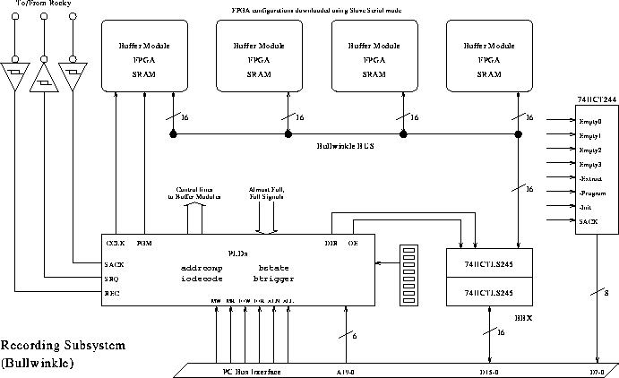
Figure 4.3: Block Diagram for Bullwinkle
The goal of the Recording Subsystem (Bullwinkle) card is to accumulate incoming data in buffer RAM and periodically save it to disk. The speed of the buffer RAM circuitry is critical because 64 bits of data come in from the ribbon cables as often as every 80 ns (assuming 25 MHz SUT speed). By using 70 ns SRAM chips and a 64 bit wide data pipeline, we should be able to achieve this goal.
The 64 bit data path is implemented using four identical 16 bit buffer modules. The FPGA-based buffer modules (Boris and Natasha) are described in detail in section 4.4.
The transfer of the data from the buffer RAM to the computer's disk must be done as fast as possible. Port I/O is unacceptably slow, so using DMA would be better. However, DMA requires the data to be read from the port into a system memory location, and then a block of memory can be dumped to disk. The usual DMA advantage of bypassing the CPU is of little concern here. The best solution is to map the card into a block of system memory locations and use normal DOS memory-to-disk block write routines. These routines are already optimized for moving data from memory to disk (using DMA, in fact). Achieving maximum speed is then a matter of making sure Bullwinkle can place a word of data on the system bus each time it decodes an address in its range without having to insert memory wait states. To the PC, Bullwinkle simply appears as a read-only memory.
Because the Intel-based PCs have segmented memory the simplest approach is to map the Bullwinkle buffer RAM into one 64k block of system memory, for example at D0000-DFFFF or E0000-EFFFF. These areas of memory are above the usual 640k main memory and below 100000 (1MB) which is the start of extended memory. DOS machines reserve the area between 640k and 1MB (A0000-FFFFF) for ROMs and memory-mapped devices, such as video memory, network cards, and other uses very similar to ours. The Bullwinkle card was tested in a machine using an ethernet card at D000 without any conflict.
The software will use I/O port writes to select which module's buffer memory to access, and perform an up to 64k byte DOS Write command from our memory segment to disk. For fastest transfer, Bullwinkle should make use of all 16 bits of the AT data bus.
The control logic for Bullwinkle resides in four AMD PALCE22V10 GALs, produced from ABEL language files addrcomp.abl, iodecode.abl, bstate.abl, and btrigger.abl. The process of compiling ABEL source into JEDEC programmer files and ViewSim simulation files, both with test vectors, is described in Appendix B.
We could put this logic in an additional FPGA, but at least one GAL would still be necessary for configuration of the FPGAs. The GALs have signals to each Boris and Natasha module for enabling, selecting recording (to RAM) or extracting (from RAM), triggering each set of recorded data, and enabling various ``local'' bus drivers and latches. The control logic GALs also get signals from Boris indicating when the RAM is Almost Full and Full.
The PC interface logic involves decoding a valid port address by comparing with DIP switch settings, and enabling bidirectional bus transceiver chips (74LS245). For a full interface description, see Section 4.5.
Handshaking logic involves asserting SRQ when the Boris modules report an Almost Full condition, and switching to Extract mode once Rocky acknowledges the Stall Request with a SACK signal. If Boris reports a Full condition before Rocky raises SACK, Bullwinkle ignores subsequent data coming in and proceeds to Extract the data to disk. While data will be missed, there is no other option, and in fact this provides a way to sample address traces instead of stalling to get a complete trace. The SACK signal is only generated if the staller program is installed on the SUT.
The FPGA configuration logic waits for a certain I/O port write upon which it provides appropriate configuration signals to the FPGAs and passes subsequent memory-written bits to the FPGAs as configuration data in Slave Serial mode. It is the reponsibility of the software to check the FPGA Init signal through an I/O port read to make sure the FPGAs are ready to be configured.
The Bullwinkle architecture allows for maximum post-construction flexibility. The board features a 16 bit B-bus, which is bidirectionally connected to the system data bus by the BBX (B-Bus Transceiver). Each buffer module has its own 16 bit local bus, which is bidirectionally connected to the B-bus by an LBX (Local Bus Transceiver), and can acquire signals from a DAR (Data Acquisition Register) connected to the ribbon cable, and connects to In/Out pins of the Boris FPGA. By enabling the appropriate combination of tri-state outputs any of the FPGAs can read from the PC data bus, from the ribbon cable, or from other buffer modules' local buses, and can write to the same (except the ribbon cable). During FPGA configuration, bit 0 of the B-bus is used for the serial FPGA bit stream.
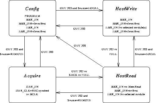
Figure 4.4: Bullwinkle State Diagram (assuming base I/O address of 300)
The Bullwinkle control GALs use a state machine which is shown in Figure 4.4. The modes HostWrite and Acquire cause identical action by Boris, that is, writing data into the SRAM until a Full condition or Stall Request. However, by alternating the Output Enable lines of the LBX and the DAR, the source of the data can either be the ribbon cable connection to Rocky ( Acquire mode) or from 16-bit writes by the host machine to the shared memory area ( HostWrite mode).
Thus the Bullwinkle architecture allows a data path that is far more flexible than the unidirectional flow implied in Figure 2.1. The ability to ``poke'' data from the PC bus into Boris and Natasha modules as if it came from the remote Rocky card will allow more extensive testing to be done without actually having another machine connected.