One main design decision was what method to use for handshaking between the Rocky and Bullwinkle cards. One possibility was to have a synchronous transmission by transmitting a clock signal across the ribbon cable. This method was ruled out in favor of an asynchronous method, which involves use of Stall Request (SRQ) and Stall Acknowledge (SACK) lines between the two cards. A synchronous system would require the handshaking signals to travel across the cable, through logic, and back before each transmission. The asynchronous tradeoff is that the Address Record pulse (REC) must be synchronized with the FPGA clock on the Bullwinkle end to prevent metastability.
In order to minimize the number of times the processor must be stalled, the system must be able to move all the addresses to be recorded into buffer memory as fast as the processor can generate them. The data path in Figure 2.1 can be thought of as a pipeline, meaning new information can be latched from the bus while the last information is still on its way to the buffers. The propagation time of each stage of the pipeline must be smaller than the minimum time between memory references by the CPU. Stall requests are generated by Bullwinkle when the buffers reach a certain ``high-water'' mark, and are propagated back to Rocky which interrupts the CPU.
We make the following reasonable assumptions as a demonstration. The
Recording PC has Memory-to-Disk transfer rate of  MB/s and
256 KB of buffer SRAM. The system under test (SUT) is a PC
running at 25 MHz and generating address references every 2 clock
cycles (maximum) and every 5 clock cycles (average). The SUT clock
period is 40 ns, so the minimum time between address references is
MB/s and
256 KB of buffer SRAM. The system under test (SUT) is a PC
running at 25 MHz and generating address references every 2 clock
cycles (maximum) and every 5 clock cycles (average). The SUT clock
period is 40 ns, so the minimum time between address references is  ns, and the average address generation rate is 5 MHz. We will
record a maximum of 64 bits of address, data, chip status, and timing
information with each reference, for a generation rate of
ns, and the average address generation rate is 5 MHz. We will
record a maximum of 64 bits of address, data, chip status, and timing
information with each reference, for a generation rate of  MB/s. Our time dilation in this case should be
 .
.
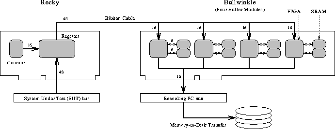
Transmitting 64 bits from the bus across a ribbon cable to Bullwinkle in 80 ns is one option, or the interface can transmit the information as two 32 bit signals in under 40 ns each. The latter option allows a smaller ribbon cable, but requires more complicated circuitry on both ends. The buffer memory on the Bullwinkle card is organized as eight 32k x 8 bit SRAMs with 70 ns access times, giving a 64 bit wide memory of 256 kB total.
One source of delay that will cut into our goal of 10% overhead is the
propagation of the asynchronous stall request and acknowledge signals.
To minimize the effect of these and other delays which occur each time
a stall happens, we must use as large as buffer as is reasonable. We
must also maximize use of the buffer by filling it as near to capacity
as possible before dumping to disk. But the high-water mark must be
low enough to prevent overflow while the Stall Request propagates back
to Rocky. The Stall signal propagation time is a
comparator delay plus line transmission time and a couple of small
logical delays, totalling under 100 ns. The dominant delay is that
between the time the interrupt signal (IRQ2) to the CPU is raised and
the time it is acknowledged via an I/O port write by the
interrupt-handling TSR program. So  (time from Stall Request
to cessation of information flow) is likely to be as much as
(time from Stall Request
to cessation of information flow) is likely to be as much as  . In this time, the buffer may receive as many as
  new address references. The high-water mark should be
comfortably smaller than 65536 - 1250. Obviously this value is SUT
dependent, and should be software selectable if possible.
new address references. The high-water mark should be
comfortably smaller than 65536 - 1250. Obviously this value is SUT
dependent, and should be software selectable if possible.
Once Bullwinkle has been signalled by Rocky that the machine is stalled, the transfer from memory to disk begins. There may be some unwanted addresses at the beginning and end of the buffer due to the interrupt handler and the CPU state being saved on the stack (in memory). The software and the Bullwinkle control logic may be able to negotiate a buffer pointer adjustment to remove this data before it gets written to disk.
The 256 kB of buffer SRAM cannot be transferred in a single memory-to-disk transfer, so the control software will make four 64 kB transfers from the D000h segment of DOS memory. It will use an I/O port write before each transfer to set which eighth of the buffer memory should be mapped to the 64 kB of system memory at D0000-DFFFF. After the final transfer, another I/O port write will clear the buffer and signal Rocky to resume execution. The port I/O time is negligible compared with the time spent on the disk transfers. The card should be designed using the full 16-bit bus width if possible to increase DMA throughput. Note that the card's shared memory page can be software-selected to the E000h segment instead if a network or other card resides at D000h.