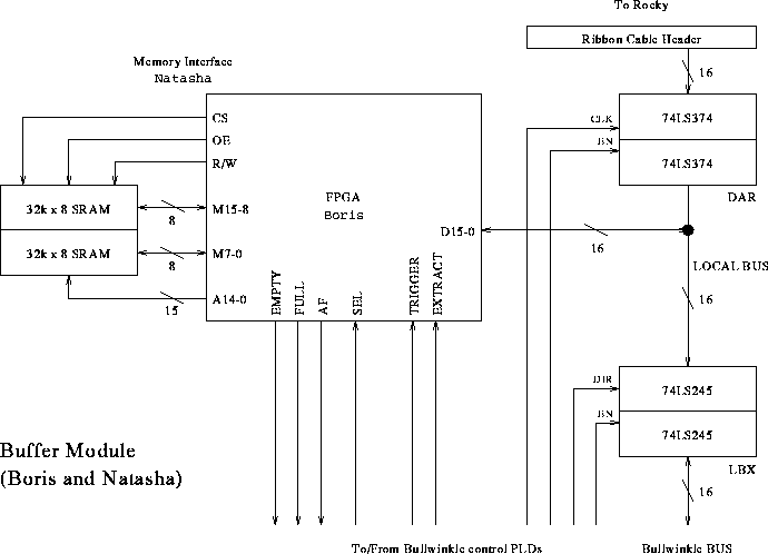
Figure 4.5: Block Diagram for Buffer Modules
As mentioned in Section 4.3, each buffer module features a 16 bit local bus connecting the FPGA, the ribbon cable input register, and the B-bus (to PC data bus and other buffer modules). The 16 bit path from the FPGA to and from the SRAM must be separate from the local bus to allow pipelining of incoming data. In addition, there is an address bus from the FPGA to the SRAM. The functionality of the address and data connections between the FPGA and the SRAM is encapsulated in the specification of Natasha. Natasha is actually just a VHDL module which gets synthesized into the FPGA alongside Boris' other data-handling functions. However, Natasha is conceptually separate in that if a different memory component (such as a FIFO or different sized SRAM) were used only the Natasha module would have to be redesigned. Also, the Natasha module will hopefully be reusable by any VHDL-based FPGA design which needs an SRAM interface.
The decision to use addressable SRAM over simpler FIFO chip buffers was based on cost and availability. However, while using FIFOs saves FPGA pins, having random-access memory adds flexibility to future designs.
The size of the SRAM was chosen to be 32k  8, and two chips are
used in each buffer module. This allows all the data from a particular
buffer module to be read in one 64k byte segment on the PC. The type of
chips used was HM62256-LP70, manufactured by Goldstar.
8, and two chips are
used in each buffer module. This allows all the data from a particular
buffer module to be read in one 64k byte segment on the PC. The type of
chips used was HM62256-LP70, manufactured by Goldstar.
The other components in each module are referred to as the DAR and the LBX. The DAR is a 16 bit register for reading values from Rocky via ribbon cable. It is two 74LS374 chips, clocked and enabled by signals from the Bullwinkle control GALs. They are be clocked synchronously with BCLK following a rising edge of REC from Rocky and enabled if Bullwinkle is in Acquire mode.
The LBX (Local Bus Transceiver) is a pair of 74LS245 bidirectional tri-state buffers. The direction and output enable lines for LBX also come from the control GALs.
The FPGA program is the top level VHDL file boris.v, with module entities specified in natasha.v and pointers.v. The FPGA must take care of matching SRAM timing specifications by using a 40 ns (25 MHz) clock and a state machine to control R/W, OE, and CS lines as well as the SRAM data and address lines. It must appropriately route the RAM data to the local bus lines or vice-versa, depending on whether Bullwinkle is extracting or recording data. It must also increment pointers into the RAM buffer for reading and writing, and using comparators signal when the pointers reach the Almost Full and Full marks.
The method chosen for maintaining read and write pointers for the SRAM was a 15-bit linear-feedback shift register (LFSR). This produces a pseudorandom sequence of 32767 addresses (the all ones state is never used). Each LFSR (one for the read pointer, one for the write pointer) is implemented as simply 15 registers and one XNOR feedback gate.
The Almost Full condition is detected by an identity comparison with a hard-coded constant address determined by the LFSR sequence generator lfsr.c. For example, to make the high-water mark equal to 75% of the SRAM's 32k capacity, we compare to the 24,575th address in the sequence, which is 17400 decimal, or 100001111111000 binary.
Empty and Full conditions both occur when the read and write pointers have the same value. The distinction is made by looking at the value of the Extract signal, since the FIFO will become Full only in Record modes and Empty only in Extract mode.
The Full flag is not checked if the write pointer was just reset to zero. After the first value is written, the read and write pointers are no longer both zero, so equality means we've wrapped around and the FIFO is truly Full.
The process for synthesizing VHDL, mapping to Xilinx format, and producing ViewSim simulation files with post-routing delay information is described in Appendix C.
Boris was tested first with only pointers implemented, and no SRAM interface. The current pointer values were routed to the Data outputs instead of the SRAM address lines, so that they could be seen by the PC. Once correct operation was observed, the SRAM interface was added to the design, resulting in the final FPGA program, natasha. This design uses 59 of the 144 available CLBs, 55 internal flip-flops, and 59 of the 74 available I/O pins. The XMAKE program took about 8 minutes.