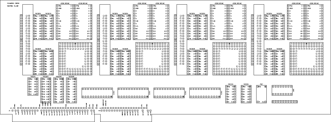
Figure 5.2: Pinouts and layout of Bullwinkle components
The layout of the Bullwinkle board is shown in Figure 5.2. Only the second buffer module (module 1) was actually wired, since modules 0, 2, and 3 are identical. The four GALs, oscillator, inverters, and system bus buffers are on the lower half of the board.
The pin assignments of the FPGA can either be specified in a constraints file or allowed to be mapped at random. A choice in between is to specify a range of pins to which a certain signal can be mapped. For example, the address lines to the SRAM were not mapped to any particular pin, but to one of a range of pins along the side and top of the package (near the SRAM). The SRAM data lines were likewise mapped to a range of pins along the top edge of the FPGA. It doesn't matter which address line on the FPGA goes to which address line on the SRAM, or which data goes to which D pin of either SRAM chip. This allows the mapping software greater flexibility in routing the desing.
Other signals, such as the main data bus and control lines, were placed to specific pins. Refer to the boris.cst constraints file in Appendix G.1.
Certain control signals from the GALs have a fan-out of up to 8 because of the repetition of buffer modules. For these signals a TTL inverter was used to improve the fan-out of the signals, and the polarity of the signals in the ABEL source was reversed.
The Init and Done/-Program configuration pins of the FPGAs are open-collector input-output pins. With multiple FPGAs, the desired signal can be obtained by wire-ANDing the signals with a pullup resistor. This allows expansion from one to multiple parallel FPGAs without additional gates. The same technique will be used for the Full and AlmostFull outputs from Boris. With only one FPGA wired, the open-collector output and pullup resistor is not a concern.
The 40-pin ribbon cable connector for each buffer module has 20 pins for data, with every other pin grounded. Resistor networks are wired between the signal lines and ground to prevent ringing due to transmission-line effects. The best values for the resistors have not yet been determined.