2.0 The SAIP HighClass Design Problem and Challenges
The BM4 SAIP HighClass processor requirements represented a typical design problem of a sophisticated signal processing application in the early stages of development. The design challenge was to demonstrate the feasibility of upgrading the current ACTD SAIP HighClass subsystem design to an affordable, tactically sized advanced development configuration. The following paragraphs provide a brief description of the SAIP System and the requirements established for the BM4 development effort.
SAIP is a DARPA ACTD program with goals of providing state-of-the-art battle awareness to the tactical field commander. The SAIP ACTD demonstration system concept is illustrated below. The operational goal of the SAIP program is to make synthetic aperture radar (SAR) imagery from airborne surveillance systems a responsive source in providing the commander with dominant battlefield awareness. The program is aimed at providing tactical information quickly to the commander regarding the enemy's ground order of battle and missile order of battle, and maintaining tactical surveillance capability of other targets of military interest.
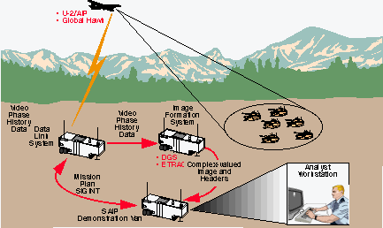
Figure 2-1 SAIP ACTD System Concept
SAIP's goals are aimed at increased image analysis efficiency. Image analysts (IAs) are automatically cued to isolated targets allowing swift human evaluation. To do this effectively, the probability of automatically, accurately detecting a target must be greater than 90% and the false alarm rate must be less than one false alarm for every hundred square kilometers.
Automatic target recognition (ATR) is the cornerstone of the SAIP system. The ACTD program brings together many existing technologies into an integrated package. SAIP integrates target recognition, cluster analysis, template based automatic target recognition, terrain analysis, object level change detection and image-to-image registration functions to achieve a high probability of detection and low false alarm rate. The baseline system uses a template-based mean square error (MSE) classifier for the SAR ATR. The SAIP performance goal of cueing IAs to isolated targets is being enhanced by high definition imaging (HDI) techniques. The HighClass processor subsystem prototype developed under BM4 implemented the SAIP HDI and MSE functions. A block diagram of the SAIP baseline system processing flow illustrates where these functions fit in the overall SAIP processing string.
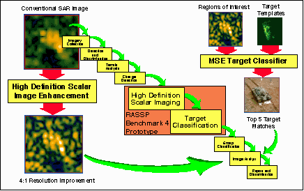
The HDI is a data-adaptive approach to SAR image reconstruction based on super resolution techniques originally developed for passive sensor arrays. The goal of HDI is twofold, namely to improve the automated recognition of the target, and aid the IA by providing an enhanced image of the target. HDI employs both amplitude and phase information . It recasts image formation as a spectrum estimation problem treating pixels as beamformer outputs. It employs algorithms such as Capon's Maximum Likelihood Method and MUSIC. It is a fully two-dimensional adaptive estimation optimized for each pixel in the output image. HDI has demonstrated improved automatic target recognition and provides sharper, more informative, imagery for the IA. (Reference 1 - Gerry Benitz's paper titled "High-Definition Vector Imaging for Synthetic Aperture Radar" published in the Conference Record of the 31st Asilomar Conference on Signals, System and Computers, November 1997.)
The SAIP MSE classifier uses a template matching algorithm to determine the five best target matches from a set of 20 possible ground order of battle target classes for specific objects of interests (image chips). It uses a two stage classifier to determine the top five target matches. In the first stage, MSE low resolution classifier (MSE-LRC), incoming image chips are correlated with all 20 low resolution target template sets. In the second stage MSE high resolution classifier (MSE-HRC), the HDI enhanced images are matched to the high resolution templates for the target classes, pose angles and dither location determined in the first stage to refine the class ordinal ranking and classification scores of the five best targets.
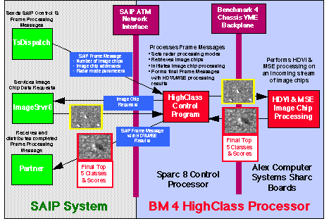
The BM4 HighClass processing subsystem effort was designed to replicate the existing SAIP HDI and MSE image chip processing functions. The prototype had to be integrated with the existing SAIP control software and data/ message structures and communicate with the SAIP system over the existing ATM communications network. The following figure provides the top level view of the required SAIP System and BM4 HighClass subsystem hardware/ software functions and interfaces.
Descriptions of the HDI and MSE algorithms were provided by MIT-LL in several forms; written documents, a non real-time C/FORTRAN code executable specification, and a Matlab simulation. MIT-LL also provided unclassified test data and a SAIP system emulator to support the software development and final system test. The functional flow and test data provided as part of the HighClass executable specification is shown in following figure.
The SAIP BM4 technical requirements were selected to demonstrate the RASSP tools and methodology innovations for developing and demonstrating a prototype of a tactically sized processor to perform the HighClass HDI and MSE ATR functions. The HighClass processor requirements represented a development challenge which was amenable to an application-specific custom processor solution for the MSE functions and COTS DSP boards for the HDI implementation.
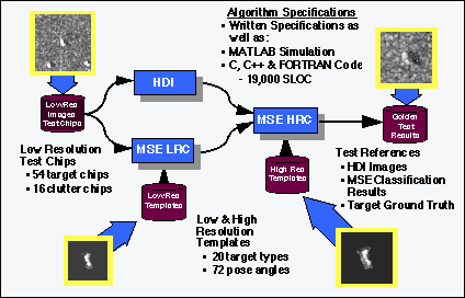
Figure 2-4 HighClass Executable Specification and Test Data
The HDI and MSE processing requirements provided significantly different challenges. The sophisticated nature of the HDI algorithms posed a complex computational problem, with a wide range of algebraic and matrix functions as well as frequency domain computations. The original implementation of the algorithms required more than 85 MFLOPS of processing for each 79x79 pixel image chip or approximately 13.6 KFLOPS per pixel. As such, the HDI processing requirements represented a complex, computation bound numerical signal processing problem for assessing the RASSP virtual prototyping and autocoding tools and methodology.
The MSE classifier used a two stage calculation to determine the best five target matches. In the first stage, the MSE low resolution classifier (MSE-LRC), correlated incoming image chips with 20 sets of low resolution target templates. Each target class is made up of 72 pose angle templates. The image chip was compared to each target pose by performing a pixel by pixel correlation between the image chip and the pose template. The correlation is performed for 121 pixel dither locations resulting in 174,240 (20x72x121) correlations per image chip. The correlation function consisted of computing and accumulating the pixel by pixel MSE score for each valid target pixel in the target template. The accumulative MSE scores for each dither location, pose angle and target class is then ordinarily ranked to determine the best five class scores. The target class, pose angle and pixel location for the five best classes are forwarded to the MSE high resolution classifier (MSE-HRC).
In the MSE-HRC, the correlation function was again computed using the HDI high resolution image chip and a set of HDI target templates to refine the final target class ranking and classification scores. Only the five best target classes were used. The number of pose angles was limited to 14 views and the number of dither locations was reduced to 49 based on the best low resolution pose angle and dither location. Again the lowest score was computed for each of the five target classes and the final rank order and scores, along with the HDI high resolution image, were output to the HighClass control processor. The figure below illustrates the functional flow for the individual image chip processing required in the BM4 HighClass prototype.
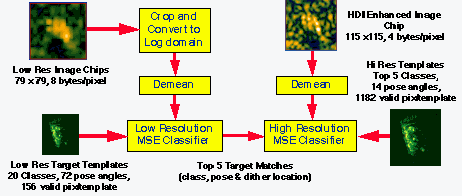
Figure 2-5 HighClass Functional Flow/Requirements
Unlike the HDI problem, the MSE classifier was a simple, highly repetitive function operating on a large quantity of template data. The MSE computation required three arithmetic operations per pixel but was performed for all dither locations, pose angles and target classes. Based on an average of 156 valid pixels per low resolution template (11,232 per target class) and 1182 valid pixels per high resolution template (16,548 per target class) a total of 84.7 MFLOPS and 12.1 MFLOPS were required for MSE-LRC and MSE-HRC respectively for each image chip. While both the HDI and the MSE classifier functions have similar throughput requirements they posed significantly different signal processing development challenges.
The individual HDI and MSE as well as the combined HighClass processing and memory requirements are summarized in Table 2 - 1. The HDI algorithm involved a complex, adaptive processing problem with moderate input/output data bandwidths, minimal data memory storage but large program/data memory requirements. On the other hand, the MSE interloop required only 3 operations per pixel for multiple target classes, pose angles and offset location. This is the same input bandwidth as HDI, an insignificant output bandwidth. The MSE function required very little program memory but needed a large amount of template data storage space. As such these two function posed dissimilar design problems with significantly different architectural requirements. Combined, the HDI and MSE processing functions provided a design problem requiring approximately, 5.36 GFLOPS of processing, 3.1 MBytes/sec input/output bandwidth, and a total processor memory requirements of 71.7 MBytes to meet the 30 chip per second, twenty target class processing requirements.
|
SAIP HDI and MSE Processing Requirements |
|||
|
HDI |
MSE |
Total |
|
|
Throughput |
|||
|
Operations per pixel (FLOPS) |
13,600 |
15,014 |
N/A |
|
Operations per Image Chip (MFLOPS) |
85.0 |
93.7 |
166.5 |
|
Operations per Second (GFLOPS) |
2.55 |
2.81 |
5.36 |
|
Input/Output Bandwidth |
|||
|
Input Bandwidth per Image Chip (KBytes) |
49.93 |
49.93 |
49.93 |
|
Input Bandwidth per second (MBytes) |
1.5 |
1.5 |
1.5 |
|
Output Bandwidth per Image Chip (KBytes) |
52.9 |
< 0.1 |
53.0 |
|
Output Bandwidth per second (MBytes) |
1.59 |
<0.003 |
1.59 |
|
Program/Data Memory |
|||
|
Data Memory Requirements (MBytes) |
0.11 |
71.6 |
71.7 |
|
Program Memory Requirement (KBytes) |
80 - 100 |
< 4 |
~100 |
Table 2-1
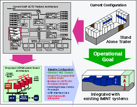
The minimum BM4 size, weight, and power requirements were 6.4 cubic feet, 250 pounds and 3 kilowatts but the design goal was to implement the BM4 HighClass subsystem in a low cost, tactically sized processor. The goal was to demonstrate the feasibility of achieving the SAIP program long term operational requirements of integrating SAIP technology into existing IMINT exploitation systems. To meet this objective, the RASSP BM4 goal was to perform the HDI and MSE processing functions 8 times faster than the current SGI processors and package the prototype in one twelfth the current volume. Resulting in a design goal of a 100X increase in processor density over the current 14 node SGI R8000architecture. To meet this objective, ATL established a design goal for a 7 board VME-6U design to achieve the BM4 program requirements.
In summary, the design problem posed by the HighClass processor development effort was to achieve 8 times the current system HDI and MSE image chip processing rate in 1/12th the size and demonstrate the feasibility of shrinking the system to allow it to be integrated with existing IMINT systems. From a top level design standpoint, this meant; performing all of the complex HDI and highly repetitive MSE processing functions on five VME-6U boards, hosting the SAIP control processor on a standard Unix board, and providing a standard ATM interface card to communicate with the SAIP system. The challenge was to accomplish the development in 9 months at a cost of less than $1.7M using the processes, tools and techniques developed under the RASSP program.
![]()
![]()
![]()
![]()
Next:3.0 The RASSP Development Process Used to Attack the Problem
Up: Case Studies Index
Previous:1.0 Introduction