CHAPTER 11 |
BRING UP AND |
We have come a long way. We have chosen or built our FPGA platform; we have manipulated our design to make it compatible with FPGA technology and we are ready with bitstreams to load into the devices on the board. Of course, we will find bugs, but how do we separate the real design bugs from those we may have accidentally introduced during FPGA-based prototyping? This chapter introduces a methodical approach to bringing up the board first, followed by the design, in order to remove the classic uncertainty between results and measurement.
We can then use instrumentation and other methods to gain visibility into the design and quickly proceed to using our proven and instrumented platform for debugging the design itself.
During debug we will need to find and fix bugs and then re-build the prototype in as short an iteration time as possible. We will therefore also explore in this chapter more powerful bus-based debug and board configuration tools and running incremental synthesis and place & route tools to save runtime.
11.1. Bring-up and debug–two separate steps?
It is worth reminding ourselves of the benefits of prototyping our designs on FPGA. We use prototypes in order to apply high-speed, real-world stimulus to a design, to verify its functionality and then to debug and correct the design as errors are discovered. The latter debug-and-correct loop is where the value of a prototyping project is realized and so we would prefer to spend the majority of our time there. It is tempting to jump straight to applying the whole FPGA-ready design into the prototyping platform, but this is often a mistake because there are many reasons why the design may not run first time, as will be discussed later in this chapter. It is very difficult in this situation to determine what prevents a design from running first time, so a more methodical approach is recommended.
When the design does not work on a prototyping board, it could be because of two broad reasons. It could be because of problems related to the prototyping board setup, or due to problems in the design that is run on the board. Separating the debugging process for these two separate problems will lessen the whole debugging time.
For effective debug-and-correct activity it is critical to make sure that the bugs we see are real design issues and not manifestations of a faulty FPGA board or mistakes in the prototyping methodology. We therefore should bring up our design step-by-step in order to discover bugs in turn as we test first the board, then the methodology and finally the completed design in pieces and as a whole. This will take more time than rushing the whole design onto the boards, but in the long run will save time and help prevent wasted effort.
These bring-up steps can be summarized as follows:
- Test the base board
- Test the base plus the add-on boards
- Apply a small reference design to single FPGA
- Apply reference design to multiple FPGAs
- Inspect SoC design for implementation issues
- Apply real design in functional subsets in turn
- Apply whole design
So, it is always necessary to make sure that the FPGA board setup is correct before testing the real design on board. The next step is to bring up the design on board by making sure that the clock and reset signals are correctly applied to the design. After the initial bring up, the actual design validation stage would start. In this design validation stage, debugging the issues becomes easy when there is enough visibility to the design internals. The necessary visibility can be brought into the design using different instrumentation methodologies which will be discussed in detail in the later part of this chapter.
11.2. Starting point: a fault-free board
We should like to start this chapter from the assumption that the FPGA board or system itself does not have any functional errors, but is that a safe assumption in real life? As mentioned in chapter 5, this book is not intended to be a manual on high-speed board design and debug so we are not intending on going into depth on board fault finding. We assume that those who have developed their own FPGA boards in house will know their boards very well and would have advanced to the point where the boards are provided, fully working to the lab.
There is an advantage at this time for those using commercial boards because these would have already been through a full-production test and sign-off at the vendor’s factory. For added confidence, board vendors should also supply user-executable test utilities or equipment in order to repeat much of the factory testing in the lab. For example, a special termination connector or automatic test program to run either on the board or on a connected host. It is not paranoid to recommend that these bare-board tests are repeated from time-to-time in order to reinforce confidence, especially when the prototype is showing some new or unexpected behavior. A few minutes running self-test might save many hours of misdirected analysis.
As well as self-test, board vendors will often provide small test designs for checking different parts of the base boards. Even if in-house boards are in use, it is still advisable to create and collect a library of small test designs in order to help commission all the parts of the boards before starting the real design debugging work.
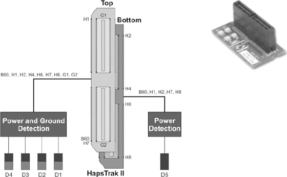
The kinds of tests applicable to a base board vary a great deal in their sophistication and scope. As an example of the low-end tests, the Synopsys® HAPS® boards have for many years employed a common interconnect system, called HapsTrak®. Each board is supplied with a termination block, called a STB2_1×1 and is pictured in Figure 133. The STB2_1×1 can be placed on each HapsTrak connector in turn in order to test for open and short circuits and signal continuity.
Figure 133 : STB2_1×1. An example of a test header for FPGA Boards
Testing the board from external connectors in this way would be a minimum requirement. Beyond this, we might also want to use any available built-in scan techniques, additional test-points, external host-based routines etc. All of these are vendor- and board-specific and apart from the simple above example, we leave it to the reader to explore the particular capability of their chosen platform. For the purpose of this manual, we will start form the previously mentioned assumption that the board itself is functional before we introduce the design. However, there are other aspects of the board and lab set-up that may be novel and worth checking before the design itself is introduced.
Typical issues that would present in the prototyping board setup are problems in the main prototyping board and daughter boards themselves, connection between these different boards through connectors and cables, or issues related to external sources like clock and reset sources. These all come down to good lab practice and we do not intend to cover those in detail here.
11.3. Running test designs
The best way to check whether the FPGA board setup is correct is to run different test designs on the board and check the functionality. By running a familiar small design which has well-known results, the correct setup of the boards can be established. Experienced prototypers can often reuse small test designs in this way and in a matter of hours know that the boards are ready for the introduction of the real SoC design.
Board vendors may also be able to supply small designs for this purpose but in-house boards will require their own tests and be tested separately before delivery to the prototypers. Use of custom-written test designs to test these boards in the context of the overall prototype can then be performed. This also applies to custom daughter boards for mounting onto a vendor-supplied baseboard. For example, if a custom board is made to drive a TFT display then a simple design might be written to display some text or graphics on a connected display in order to test the custom board’s basic functionality and its interface with the main board.
In either case, it is recommended to connect all the parts of the prototype platform including the main board, daughter boards, power supply, external clocks, resets, etc. as they will be used during the rest of the project. Then configure the assembled boards to the exact setting with which the actual design will employ during runtime, including any dip switches and jumpers. Sometimes these items can be controlled via a supervisory function which will access certain dedicated registers on the board under command of a remote-host program. It is especially important to configure any VCO or PLL settings and the voltage settings for each of the different IO banks of the FPGAs. Off-the-shelf prototyping boards like the HAPS board provide an easy way of configuring this using dip switches and on-board supervisory programs.
We are then ready to run some pre-design tests to ensure correct configuration and operation of the platform. Here are some typical test designs and procedures which the authors have seen run on various prototyping boards.
- Signs-of-life tests are very simple. Reading or writing to registers from an external port can confirm that the FPGA itself is configuring correctly.
- Counter test to test clocks and resets are connected and working correctly. Write a simple counter test-design with the clock and reset as inputs and connect the outputs to LEDs or FPGA pins which connect to test points in the board, or read the counter register using an external host program.
- Daughter board reference designs provided by vendors or equivalent user-written test designs can be used to check the functionality of the addon daughter boards. Testing with these designs would test the proper functionality of the daughter boards and the interface between the main board and the daughter boards and links to external ports, such as network analyzers.
- High-speed IO test: If the prototyping project makes use of advanced inter FPGA connectivity features like pin multiplexing or high-speed time division multiplexing (HSTDM), it is advisable to run simple test designs to test this on the board. Owing to the environmental dependency of LVDS and other high-speed serial media the test designs should employ the same physical connections in order to properly replicate the final paths to be use in the SoC prototype.
- Multi-FPGA test designs: If the design is partitioned across multiple FPGAs, then it is advisable to test the prototyping board with a simple test design which is easily partitioned across all the devices. One example of this would be an FIR filter with each tap partitioned in a different FPGA. Let’s look at that example in a little more detail.
11.3.1. Filter test design for multiple FPGAs
One example of a simple-to-partition design which tests many aspects of a multi-FPGA design configuration is the FIR shown in Figure 134 which would serve to test four FPGAs on a board.
Figure 134 : A 4-tap pre-loadable transposed FIR filter test design
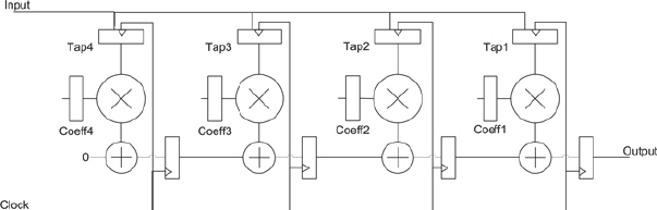
An FIR, being a fully synchronous single-clock design helps to check that reset timing is correct and that clock skew is within an acceptable range.
Figure 135 : RTL code for FIR filter test design
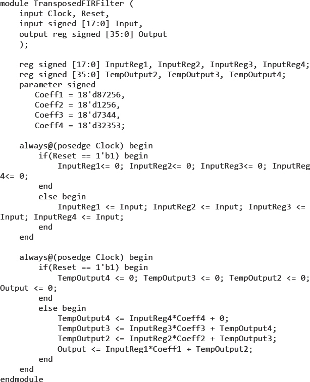
The RTL for this design is seen in Figure 135 and this may be synthesized and then split across four FPGAs either manually or by using one of the automated partitioning methods discussed earlier. The values of the coefficients, although arbitrary, should all be different.
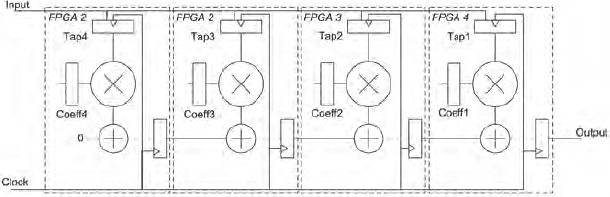
The design is partitioned so that each tap (i.e., multiplier with its coefficient and adder) is partitioned into its own FPGA, as shown in Figure 136. Care should be taken with FPGA pinout and use of on-board traces to ensure that connectivity between the FPGAs is maintained.
Figure 136 : FIR filter test design partitioned across 4 FPGAs
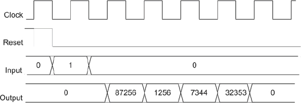
A logic analyzer is connected at the output and a pattern generator is connected at the input. Once the design is configured into the FPGAs then it can be tested by applying an impulse input as shown in Figure 137. The pattern generator can be used to apply the impulse input. An impulse input consists of a “1” sample followed by many “0” samples. i.e., for 8-bit positive integer values, then the input would be 01h for one clock followed by 00h for every clock thereafter. As an alternative to using an external pattern generator, a synthesizable “pattern generator” can be designed in one of the FPGA partitions to apply the impulse input. This is a simple piece of logic to provide a logic ‘1’ on the least significant bit of the input bus for a single clock period after reset.
The expected output from FPGA4 should be the same as the chosen filter coefficients and they should appear sequentially at FPGA4’s output pins as the pulse has been clocked through the filter (i.e., one clock after impulse input has applied in this 4-tap example), as shown in Figure 137.
11.3.2. Building a library of bring-up test designs
As the team becomes more familiar with FPGA-based prototyping, common test designs will be reused for different prototypes. It is advisable to create a way to share test designs amongst team members and across different projects. Creating a reusable test infrastructure with a library of known good tests usable on different boards is an investment that will benefit multiple prototyping projects and increase efficiency of our FPGA-based prototyping. This library could be considered in advance, or gradually built up with each new prototyping project.
Figure 137 : Expected FIR behavior across four FPGAs
By running such simple designs on the prototyping board setup, the whole setup is tested for its basic functionality and we get comfortable with the FPGA-based prototyping flow. After running few designs on the board, we would know how to partition a design, synthesize and place & route them, create bit files, program the FPGAs with the bit files and do some basic debugging on the board. This knowledge would help us while debugging the real design on the board setup.
By testing this design on board, we become familiar with the complete flow of partitioning a design across multiple FPGAs, managing the connections between them and running them on board. In fact, during early adoption of FPGA-based prototyping by any project team, this type of simple design is good for pipe-cleaning methods to be used in the whole SoC design later.
11.4. Ready to go on board?
At this stage, some teams will decide to introduce the SoC design onto the FPGA board. It may have seemed like a long time to finally reach this stage but an experienced prototyping team will perform these test steps discussed in section 10.1 in a few hours or days at most. As mentioned, a piecemeal approach to bring-up may save us a great deal of false debug effort.
There is one further step which is recommended for first-time prototypers or any team using a new implementation flow and that is to inspect the output of the implementation flow back in the original verification environment. Our SoC design has probably undergone a number of changes in order to make it FPGA-ready, not least, partitioning into multiple devices. There may be other more subtle changes that may have crept in during the kind of tasks described in chapter 7 of this book. How can we check that the design is still functionally the same as the original SoC, or at least only includes intentional changes? The answer is to reuse the verification environment already in use for the SoC design itself.
11.4.1. Reuse the SoC verification environment
As mentioned in chapter 4, the RTL should have been verified to an acceptable degree using the simulation methods and signed off as ready for prototyping by the RTL verification team. Their “Hello World” test will probably have already been run upon the RTL and it is very helpful if this same test harness can be reused on the FPGA-ready version of the design.
We have seen that by reusing the existing SoC test bench we can identify differences between the behavior of the design before and after the design is made ready for the prototype. It is important that any functional differences between the SoC RTL and the FPGA-ready version can be accounted for as either intentional or expected. Unexpected differences should be investigated as they may have been introduced while we were preparing the prototype, often in the implementation process.
11.4.2. Common FPGA implementation issues
Despite all our best efforts, initial FPGA implementations can be different to the intended implementation. The following list describes common issues with initial FPGA implementations:
- Timing violations: timing analysis built into synthesis and place & route tools operates upon each FPGA in isolation. Timing violations across multiple FPGAs, for example, on paths routed through FPGAs or between clock domains in different FPGAs, would not be highlighted during normal synthesis and place & route.
- Unintended logic removal: it may not be obvious at first, but modules and IO seem to “disappear” from the resulting FPGA implementation due to minimization during synthesis. The common cause is improper connectivity or improper modules and core instantiations that result in un-driven logic, which is subsequently minimized. Early detection of accidental logic removal can save valuable FPGA implementation time and bench debug time. A review of warnings and the FPGA resource utilization, especially IO, after design co mpletion will indicate unintended logic removal, for example if there is a sudden unexplained drop in IO.
- Improper inter-FPGA connectivity: despite all efforts, due to improper pin location constraints, the place & route process will assign IO to unintended pins resulting in unintended and incorrect inter-FPGA connectivity. This often happens the first time a design is implemented or drastically modified. The remedy for this issue is to carefully examine the pin location report generated by the place & route tools for each FPGA and compare against the intended pin assignments.
Let’s consider each of these types of implementation issues in more detail.
11.4.3. Timing violations
The design may have timing violations within an FPGA or between FPGAs. It is always advisable to run the static timing analysis with proper constraints on the post place & route netlist and make sure that all timing constraints are met. Even though FPGA timing reports consider worst case process, voltage and temperature (PVT) conditions, if timing constraints as reported by the timing analysis are not met, there is no guarantee the design will work on board.
Here are some common timing issues we might face while analyzing timing on a design and some tips on how to handle them:
- Internal hold time: if we are prototyping the design at a very slow clock rate then we might be tempted to think that there cannot be timing violations on today’s fast FPGAs. As a result we might not choose to run full timing analysis. However even in such scenarios, there can be hold time violations which will prevent the design from working on board. So, even if the timing requirements are very relaxed, FPGA internal timing should be analyzed with appropriate constraints and with the use of minimum timing models.
- Inter-FPGA delays: careful analysis of inter-FPGA timing, taking in account board delays, should be made to ensure inter-FPGA setup and hold times are met. For this we need to know the appropriate board and cable delays to account for these either within the timing model or by setting appropriate constraints for whole-board timing analysis. If off-the-shelf standard prototyping boards and their associated standard cables are used for inter-FPGA connection then the expected board and cable delays should be available from the vendors. For example, the Synopsys HAPS series boards are designed to have track delays matched across the boards and between boards and delays are specified in terms of two constants, X and Y. We referred to these X and Y delay specs in the PLL discussion in section 5.3.1 and for a HAPS-54 boards for example the nominal values are X=0.44ns and Y=1.45ns. These values can be used to add delays into calculations for inter-FPGA delays.
- It is an advantage if the boards are pre-characterized for use in timing analysis tools, as is the case for HAPS boards in the Certify® built-in timing analyzer. If a custom-made board or manual partitioning is used then whole-board timing analysis would be more complex but could still be done as long-delay data could be provided by the PCB development and fabricat ion tools.
- Timing complexity of TDM: If the prototype uses pin multiplexing to share one connection between FPGAs for carrying multiple signals, then the effect of this optimization on the inter-FPGA timing should be analyzed carefully. See chapter 7 for more consideration of the timing effects of signal multiplexing.
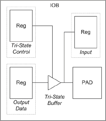
- Input and output timing: constraints on all the FPGA ports through which the design interacts with the external world should not be neglected. Without proper IO constraints, the interface with the external peripherals may not work reliably. Timing is easier to meet if the local FF features of the FPGA’s IO buffers are used to their full extent, thus removing a potentially long routing delay from an internal FF to reach the IO Blocks (IOBs). As was shown in chapter 3, all the IOBs of the FPGAs have dedicated FFs for data input, output and tri-state enables. These FFs should be used by default by the synthesis and place & route tools, but may require some intervention using the tool-specific attributes.
If the FFs have not been used properly during the implementation flow then timing problems may be introduced. For example, consider the simplified view of a typical FPGA IOB shown in Figure 138 and its use as a tri-state output pin. The recommendation is to use the FFs available in IOB for both the tristate control path and the output datapath. For tristate signals, timing advantage of using the IOB FF can be realized by using both the tri-state FF and output data FF. If neither FF is used then the extra routing delay in that path will nullify the timing advantage obtained in the other path.
For example, if the output path uses its IOB FF and the tristate control path does not use its FF then the output data may indeed arrive sooner at the tri-state buffer. The output data would only reach the PAD after the tri-state control reaches the tri-state buffer and after that buffer’s switch-on delay. In effect, the timing advantage produced by using the IOB FF in the datapath is offset by the non-optimal delay in the tri-state control path.
Similarly, if the tri-state control path uses the IOB FF and output datapath does not use its FF then the tri-state buffer will put the previous output FF data at the output PAD when the tri-state control is asserted and after a little while the new data will arrive at the output PAD. This skew in the arrival time of tri-state control and data may introduce glitches at the PAD output which may or may not be tolerable at the external destination.
Figure 138 : Typical FF arrangement in an FPGA IO cell
- Inter-clock timing: as is true for all logic design, we should take special care with multi-clock systems when signals traverse between FFs running in different clock domains. If the two clocks are asynchronous to each other then there can be setup and hold issues leading to metastability (check references for more background on metastability). Avoiding metastability between domains is as much a problem in FPGA as it is in SoC design so similar care should be taken. In fact, the measures taken in the SoC RTL to avoid or tolerate metastability (e.g., double-latching using two FFs in series on the receiving clock) can be transferred directly into the FPGA but we should also apply all the timing constraints used for ASIC to the FPGA.
- We can ensure that the probability of meta-stable states is within reason or otherwise take counter-measures. In either case we should reassure ourselves that the problem is under control before going onto the board. Timing analysis for each FPGA may indicate where metastability can occur. For example, Synopsys FPGA synthesis tools generate specific warning messages for signals traversing clock domain boundaries and these messages can be checked manually or by a script. This becomes more complex when analyzing multiple FPGAs. One suggestion is to avoid setting partition boundaries so that the sending FPGA and receiving FPGA are on different asynchronous clocks.
- Gated clock timing: if there are gated clocks in the design which are not converted then there is potential for hold-time violations to occur inside the FPGAs, caused by clock skew and possibly even glitches on poorly constructed clock gates (although the latter is a real bug and good to feed back to the SoC team). Preferably all gated clocks will have been converted using techniques discussed in chapter 7, but it is possible that some have been omitted or not converted correctly leading to timing issues after place & route. Close inspection of the synthesis tools report files for messages regarding the success or failure of gated-clock conversion can often give clues to the cause of unexpected timing violations.
- Internal clock skew and glitches: we should be using the built-in global and regional clock networks which are inherently glitch free. Check for low-fanout clocks that have been accidentally mapped to non-global resources.
- Timing on multiplexed interconnect: as we saw in chapter 8, the timing of TDM connections between FPGAs can be crucial. We need to ensure that the timing constraints on both the design clock and the transfer clock are correct and confirm that they are met by performing the post place & route timing analysis. It is especially important to re-confirm that the time delay between design and transfer clock is within limits, that the on-board flight time is not longer than expected, and that, if asynchronous TDM is in use, synchronization has been included between the design and transfer clock domains.
We can see from these examples above that thorough timing analysis of the whole board is very useful and can discover many possible causes of non-operation of a prototype before we get to the stage of introducing the design onto the board. Any of these timing problems might manifest themselves obscurely on the board itself and potentially take days to uncover in the lab.
11.4.4. Improper inter-FPGA connectivity
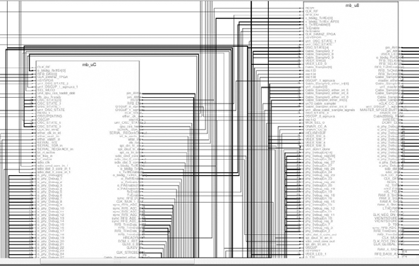
Another difficult-to-find problem is improper connectivity between the FPGAs on the board. That is, signals between FPGAs which are misplaced so that the source and destination pins are not on the same board trace. Keeping correct contiguity between FPGA pins should be a matter of disciplined specification and automation. However, as the excerpt from a top-level partition view in Figure 139 shows us (or rather scares us), there will be thousands of signal-carrying pins on the FPGAs in a typical sized SoC prototype. If any one of these pins is misplaced (i.e., the signal is placed on the wrong pin) then the design will probably not behave as expected in the lab and the reason might prove very hard to find.
If this happens then it is most likely during a design’s first implementation pass or after major RTL modification or addition of new blocks of RTL at the top level.
Figure 139 : Certify® Partition View illustrating complexity of signals between FPGAs
Pin location constraints are passed through different tools in the flow, usually from the partition tool to the synthesis tool to the place & route tool. If any of the different tools in the flow drops a pin location constraint for some reason then the place & route tool will randomly assign a pin location with only low probability that it will be in the correct place. The idea of pin placements being “lost” might seem unlikely but when a design stops working, especially after only a small design change, then this is a good place to look first.
Possible reasons for pin misplacement include accidentally setting a tool control to not forward annotate location constraints. Another mistake is to rely on defaults that change from time-to-time or over tool revisions. A further example happens when we add some new IO functionality but neglect to add all of the extra pin locations. In every case, however, we will notice the missing pin constraints if we look at the relevant reports.
We should carefully examine the pin location report generated by the place & route tools for each FPGA and compare against the intended pin assignments. In the case of the Xilinx® place & route tools, this is called a PAD report. Human inspection of such reports, which can be many thousands of lines long, might eventually lead to an error so some scripting is recommended. The script would open and read the pin location reports and look for messages of unplaced pins but while doing so, could also be looking for other key messages, for example, missed timing constraints or over-used resources. In the case of the pin locations, we might maintain a “golden” pin location reference for all the FPGAs so that the script can automatically compare this against the created PAD reports after each design iteration. This would add an extra layer of confidence on top of looking for the relevant “missing constraint” message. In addition, we could set up other scripted checks in order to compare any pin location information at intermediate steps in the flow, for example, between the location constraints passed forward by partition/synthesis to the place & route, and those present in the final PAD files.
It is worth noting that if a commercial partitioning tool is used then inter-FPGA pin location constraints should be generated automatically and consistently by the tool, perhaps on top of any user-specific locations. In the case of Certify, if the connectivity in the raw board description files are correct and the assignments of all the inter FPGA signals to the board traces are complete then there is a very minimal risk that the pin locations will be lost of misplaced by the end of the flow.
On the other hand, if we manually partition the design, then we need to carefully assign the pin location constraints for all the individual inter-FPGA connections as well as make sure that these are propagated correctly to the place & route stage, which can become a tedious and therefore error-prone task if not scripted or otherwise automated.
If all this attention to setting and checking pin locations seems rather paranoid then it is worth remembering that there might be thousands of signals crossing between FPGAs. In the final SoC, these signals will be buried within the SoC design and the verification team will go to great lengths to ensure continuity both in the netlist and in the actual physical layout. A single pin location misplacement on one FPGA would be as damaging as a single broken piece of metallization in an SoC device and perhaps harder to find (albeit easier to fix). Therefore it pays to be confident of our pin locations before we load the design into the FPGAs on the board.
11.4.5. Improper connectivity to the outside world
As well as between FPGAs, we need the proper connectivity between the FPGAs and any external interfaces. Some of the simplest but most crucial external interfaces are clock and reset sources, configuration ports and debug ports. The more sophisticated connections would be interfaces to external components like DDR SDRAM, FLASH and other external interfaces.
Once again, the implementation tools rely on there being correct and complete information about physical on-board traces between the FPGAs and from the FPGAs to the external daughter cards which may house the DDR etc. On a modular system, with different boards being connected together, the board description will be a hierarchy of smaller descriptions of the sub-systems and wit h a little care, we can easily ensure that the hierarchy is consistent and that the sub-boards are themselves correctly described. It may be worthwhile to methodically step through the board description and compare it to the physical connection of the boards, however, some systems will also allow this to be done automatically using scan techniques to interrogate each device on the boundary scan chain and check that they appear where they should, according to the board description.
A commercial board vendor will be able to provide complete connection information for the FPGA boards and for their connection to daughter boards for this purpose. In such a board description, inter-FPGA connections on the board will be labeled generically because they might conceivably carry any signal (or signals) in the design.
For connections to dedicated external interfaces, however, the signal on each connection is probably fixed e.g., a design signal called “acknowledge” must go to the “ack” pin on the daughter card’s test chip. In those cases, it can help to also give the traces in the board description the same meaningful name to make it is easier to verify the connectivity to external interfaces and match signals to traces. So for example, we can easily check that a trace called “ack” on the board is connected to a pin called “ack” on the daughter card and is carrying a signal called “ack” from the design. This naming discipline is especially useful for designs with wide bus signals.
Some advanced partitioning tools will be able to recognize that signals and traces, or signals and daughter-card pins, have the same name and therefore quickly make an automatic assignment of the signal to the correct trace, which if the board description is correct, will automatically also assign the signal to the correct FPGA pin(s). All of our pin assignments would therefore be correct by construction.
11.4.6. Incorrect FPGA IO pad configuration
When connecting various components at the board level, care must be paid to the logic levels of all interconnecting signals and be sure they are all compatible at the interface points. As well as having the correct physical connection, the inter-FPGA signals and those between the FPGAs and other components must be swinging between the correct voltage levels. As we saw in chapter 3, FPGA cores run at a common internal voltage but their IO pins have great flexibility and can support multiple voltage standards. The required IO voltage is configured at each FPGA pin (or usually for banks of adjacent pins) to operate with required IO standards and is controlled by applying the correct property or attribute during synthesis or place & route.
This degree of flexibility must be controlled because a pin driving to one voltage standard may be misinterpreted if interfacing with a pin set to receive in a different standard. This may seem obvious but as with the physical connection of the pins, the scale of dealing with voltage standards on thousands of signals adds its own challenge. For all the inter-FPGA connections, the IO standards of the driving FPGA pin and the driven FPGA pin should be the same.
The partition tools should automatically take care of assigning the same IO standards for connected pins, or warning when they are not. The default IO standard for the synthesis and place & route may also suffice for inter-FPGA connections but it is not recommended to rely only on default operation. In addition, care should be taken when the design is manually partitioned.
The board-level environment may also constrain the voltage requirement and we will need to move away from the default IO voltage settings. Then there are special considerations for differential signals compared with single-ended.
Let’s look at some of these board-level voltage issues here:
- The correct IO standard for differential signals: on a prototyping board, it is likely that only a subset of traces can be used in differential mode. Not only must pin location constraints be correct to bring signals to the correct FPGA pins to use these traces but also the pin’s IO standard must be set correctly. It is a subtle mistake to have a differential signal standard at one end and single-ended standard at the other, so that even though the pins are physically connected, the signal will not pass correctly between FPGAs.
- Voltage requirements for peripherals: for all the connections with external chips and IOs, we should first identify the IO standard of the pins of the external chips and IOs and then apply the same IO standards for the corresponding FPGA pin connected.
- IO voltage supply to FPGA: while configuring a certain IO standard for a certain pin in an FPGA, we should connect the necessary voltage source to the VCCO pins and VREF pins of the FPGA’s corresponding IO bank. As discussed in chapters 5 and 6, the boards must have the flexibility to be able to switch different voltage supplies to different banks. We must then make sure that proper supply voltages are connected to all the VCCO pins according to the chosen IO standards. This is usually a task of setting jumpers or switches or, in some cases, of using a supervisor program to control on-board programmable switches, as seen in chapter 5.
- Termination settings: some of the IO standards require appropriate termination impedance at the transmitting and receiving ends. The FPGA’s IO pads can be configured for different kinds of terminations and different impedances, for example using the digitally controlled impedance (DCI) feature in Xilinx® FPGAs. Once again, it is worth a quick check at the end of the flow to make sure that these are configured as expected.
- Drive current: the ports in the FPGA which interact with external chipsets should be able to source or sink the required amount of drive current as specified in the data sheets of the external chipsets. The FPGA’s IOs can be configured to source and sink different currents, for example on normal LVCMOS pins on a Virtex®-6 FPGA, this can be programmed to be between 2mA and 24mA. This would have already been considered during the early stages of the prototyping project but it is important that the FPGA pins be configured to supply the current or else inconsistent performance will result. This is one of those user-errors that can remain hidden for much of the project as in lab conditions we might be lucky while the peripheral is not running at full spec or otherwise does not demand full current from the FPGA pin. However, at other times the behavior of the design might become inconsistent for no apparent reason because the software might be using a feature of the peripheral not previously enabled.
- Poor signal integrity: commercial prototyping boards typically have acceptable point-to-point signal integrity at the board level. the same board design will probably have been previously used for multiple designs worldwide. However, first time we use a custom-built boards we may need some careful analysis and debug for such issues. Even off-the-shelf systems can exhibit poor signal quality with “exotic” connectivity, for example, when creating buses shared by multiple FPGAs or cables that are too long or not properly terminated. It is always best to identify and fix the root causes when possible before programming the board with the real DUT. For marginal noise or signal quality issues, we can sometimes change the programmable slew rate and drive strength at the FPGA IO pin.
11.4.6.1. NOTE: run scripts to check IO consistency
Although most of the inter-FPGA IO considerations above will be managed by the partitioning tools and therefore consistent by construction, we should maintain a “golden” reference for IO standard, voltage, drive current and placement for the critical pins on the FPGA and certainly between the FPGAs and external peripherals. We can then compare the golden reference against the created PAD report for each FPGA, however, it is wrong to have to make repetitive manual checks on every iteration of the design, so it is worth taking the time to script these kinds of checks.
We have mentioned how scripts can be used to automate these post-implementation, pre-board checks. Tools will have their own commands for generating reports on a large number of details, including top-level ports. A script can make mult iple checks on such reports in the same pass, for example verifying that the IO standards could be combined with the pin location constraints, checking that every top-level port or partition boundary signal has an equivalent entry in the FPGA location constraints. Automatically running these scripts in a larger makefile process will prevent running on into long tool passes using data that is incomplete, and wasting a lot of time as a result.
11.5. Introducing the design onto the board
Once we are confident that the platforms/boards are functional and we are confident of the results of our implementation flow then we can focus on introducing the FPGA-ready version of the SoC design onto the board.
This first introduction should be done in stages because it is unlikely that every aspect of the design’s configuration will be correct first time. Some configuration errors have an effect of masking others and so bringing up the prototype in stages helps to reduce the impact of such masking errors.
After checking the prototyping board setup with some test designs and verifying that there are no FPGA implementation issues, the actual design to be prototyped can be taken to the board. Here are some useful steps to follow:
- Confirm that the prototyping board setup is properly powered up before programming the FPGAs. Then we can program all the FPGAs with the corresponding generated bit files. Please refer to FPGA configuration in the chapter 3 and external references noted in the appendices for further details on configuring the FPGAs. There are dedicated “DONE” pins in all Xilinx® FPGAs which get asserted when the FPGAs are programmed successfully. In off-the-shelf prototyping boards like HAPS boards, these DONE pins are connected to LEDs on the boards so that the LEDs glow when the FPGAs are programmed successfully. It is advisable to check and make sure that all these LEDs glow to indicate the success of programming all the FPGAs. During configuration, some FPGAs can draw their peak current, owing to the large number of elements switching inside the device fabric. This peak may be high enough to overload the board’s power supply. This is not to say the power distribution to the devices which should have been considered by the board developers long before its use in the lab. A more common power supply error during configuration is to have current limit on the lab power source set too low, leading to voltage rail brown-out during configuration.
- After programming the FPGAs and releasing the reset, it is worth doing a simple check to see that voltage rails are sound while the FPGAs are running. Some power supplies can power the bare prototyping boards but not when a real design is running on the FPGAs. Some commercial prototyping boards such as HAPS have built-in “power good” indicators and voltage sensing components which can be read by a supervisory program to help in this task.
- Initial checks can be performed at the inputs and outputs of the FPGAs and external components. Checking the inputs first makes sense and if these are valid, then move on to the FPGA outputs. Some of the inputs which need to be checked first are the clock and reset inputs, especially those which are derived inside other the FPGAs. The inputs which are driven by any external chipsets should also be checked. Sometimes there are circular dependencies which can prevent start-up of the SoC design in FPGA. For example, the reset for one FPGA is driven by logic in another which depends upon a signal driven from the first FPGA.
- If all the inputs are valid then we can check all the outputs from the FPGAs and this leads us onto the subject of probing the FPGA. This is covered in depth in the next section.
- If the design spans multiple FPGAs, then start the debugging by checking the functionality of the parts of the design which reside in a single FPGA. This will eliminate the possibilities of problems in the inter-FPGA connections, complex pin multiplexing schemes, cables, connectors and traces on the prototyping boards.
- If the design has lot of interactions with external chip sets and IOs, then test all the parts of the design which reside only inside the FPGAs initially. This will eliminate the possibilities of problems in the external chipsets and problems occurring in the interactions.
11.5.1. Note: incorrect startup state for multiple FPGAs
A common issue with multi-FPGA systems is the improper startup state. In particular, if the FPGAs do not all start operating at the same time, even if they are only one clock edge apart, then the design is very unlikely to work.
Consider the simple case of a register-to-register path sharing a common clock. If the source and destination registers are partitioned into separate FPGAs and the receiving FPGA becomes operational just one clock cycle after the sending FPGA, then the first register-to-register transmission will be lost. Conversely, if the sending FPGA becomes operational one clock later than the receiving register, then the first register-to-register data may be random and yet still be clocked through the receiving FPGA as valid data. This simple example shows how there might be coherency problems across FPGA boundaries right from the start. These startup problems can also occur between FPGAs and external components such as synchronous memories or sequenced IOs.
A number of factors determine the time it takes for an FPGA to become operational after power up or after an external hard reset is applied, and it can vary from one FPGA to another. Prime examples are clocking circuitry (PLL/DCM) that use an internal feedback circuit and can take a variable amount of time to lock and provide a stable clock at the desired frequency. In addition, any hard IO such as Ethernet PHY or other static hardware typically becomes operational much sooner than the FPGAs as they do not need to be configured.
When the design shows signs of life but not as we know it, then one place to look is at this startup synchronization.
The remedy for the synchronized startup condition issue is a global reset management, where all system-wide “ready” conditions are brought to a single point and are used to generate a global reset. This is covered in detail in chapter 8.
11.6. Debugging on-board issues
After giving ourselves confidence that the FPGA board is fully functional and configured correctly, and also having checked the implementation and timing reports for common errors, we can consider that our platform is implemented correctly. From here on, any functional faults in the operation of the design will probably be bugs in the design itself that are becoming visible for the first time. The prototype is starting to pay us back for all our hard work.
The severity and number of the bugs discovered will depend upon the maturity of the RTL and how much verification has already been performed upon it. We shall explore in the remainder of this chapter some common sources of faults.
11.6.1. Sources of faults
Every design is different and we cannot hope to offer advice in this manual on which parts of the design to test first or which priority to place on their debug. However, we can offer some guidance on ways to gain visibility into the behavior and some often-seen on-board problems.
Assuming the design was well verified before its release to use, we should be looking for new faults to become evident because the design on the bench is exposed to new stimulus, not previously provided by the testbench during simulation. The cause of such faults can be found in three main areas, as listed in Table 29.
Table 29: Three main kinds of SoC bug discovered by FPGA-based Prototyping
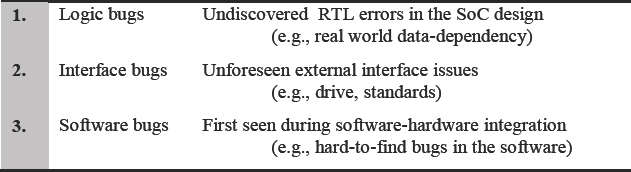
Type 1 bugs should be caught by the normal RTL verification plan and as mentioned previously, an FPGA-based prototype is not the most efficient way to discover RTL bugs, especially when compared to an advanced verification methodology like VMM. Nevertheless, RTL bugs do creep into the prototype either because there is an unforeseen error exposed by real-world data or because the RTL issued to the prototyping team is not fully tested.
Type 2 bugs are related to the SoC’s interface with external hardware. All SoC’s are specified to be used in a final product or system but there is a diminishing return on making specifications ultra-complete. Eventually there may be some combination of external components that do not fit within the spec and the design needs to be altered to compensate. This is often the case when extensive use of IP means that the SoC is the first platform in which a certain combination of IP has ever been used together. Alternatively, the design itself may be an IP block that is being specified to run in a number of different SoC designs for different end-users. Predicting every possible use of the IP is hard and corner cases are often discovered during the prototyping stage.
Type 3 bugs are the most valuable for the prototyping team to find. The prototype is the first place where the majority of the embedded software runs on the hardware. The interface between software and hardware is very complex having time dependency, data dependency and environmental dependency. These dependencies are difficult to model properly in the normal software development and validation flows, therefore on introduction to real hardware running at (or near) real-speed, the software will tend to display a whole new set of behaviors.
Any particular fault may be a combination of any two or indeed all three types of bug, so where do we start in debugging the source of a fault?
11.6.2. Logical design issues
Assuming that our newly found bug is not a known RTL problem, already discovered by the verification team since delivering the RTL for our prototype (always worth checking), we now need to capture the bug. We need to trace enough of the bug-induced behavior in order to inform the SoC designers of the problem and guide their analysis. This means progressively zeroing-in on the fault to isolate it in an efficient and compact form for analysis, away from the prototype if necessary.
The first step in identifying the fault is to isolate it to the FPGA level. To accomplish this, we need visibility into the design as it is running in the FPGAs. As mentioned in chapters 5 and 6, it is good practice to provide physical access to as many FPGA pins as possible so that they can be probed with normal bench instruments such as scopes and logic analyzers. Test points or connectors at key pins will hopefully have been provided by the board’s designers for checking key signals, resets, clocks, etc. However, most FPGA pins will usually be unreachable, being obscured as they are by the FPGAs ball grid array (BGA) package and therefore we need some other form of instrumentation.
The simplest type of instrumentation is to sample the pins of the FPGA using their built-in boundary scan chains, often referred to by the name of the original industry body that developed boundary scan techniques, JTAG (Joint Test Action Group). FPGAs have included JTAG chains for many years, primarily to assist test during manufacture and ensuring sound connection for BGAs. JTAG is most commonly known to FPGA users as one of the means for configuring the FPGA devices via a download cable. JTAG allows the FPGA’s built-in scan chains to be used to drive values from the FPGA pins internally to the device and externally to the surrounding board. Through intelligent use of the JTAG chains and intelligent triggering of the sample by visible on-board events, a JTAG chain can capture a series of static snapshots of the pin values, helping to add some visibility to a debug process.
Greater visibility at FPGA boundaries or at critical internal nodes is provided by instrumentation tools such as ChipScope and Identify as described in chapter 3. As with any of these tools, there is an inverse correlation between how selective we are in our sampling ‘vs’ the amount of sample data. Since data is usually kept in any unused RAM resources available in the FPGA, we should expect that we will not be able to capture more than a few thousand samples of a few thousand nodes in the FPGA. Therefore we need to use some of our own intelligence and debug skills in order focus the instrumentation on the most likely sites of the fault and its causes.
A good Design-for-Prototyping technique is for the RTL writers to create a list of the key nodes in their part of the design i.e., a “where would you look first” list. This list would be a useful starting point for applying our default instrumentation.
11.6.3. Logic debug visibility
There is a traditional perception that FPGA-based prototyping has low productivity as a verification environment because it is hard to see what is happening on the board. Furthermore, the perception has been that even when we can access the correct signals, it is difficult to relate that back to the source design.
It is certainly true that FPGA-based prototypes have far lower visibility than a pure RTL simulator, however, that may be the wrong comparison. The prototype is acting in place of the final silicon and as such it actually offers far greater visibility into circuit behavior than can be provided from a test chip or the silicon itself. Furthermore the focus of any visibility enhancement circuits can be changed, sometimes dynamically.
As a short recap on the debug tools explored in chapter 3, we can gain visibility into the prototype in a number of ways; by extracting internal signals in real-time and also by collecting samples for later extraction and analysis.
Real-time signal probing: in this simplest method of probing designs’ internal nodes, we directly modify the design in order to bring internal nodes to FPGA pins for real-time probing on bench instruments such as logic analyzers or oscilloscopes. This is a common debugging practice and offers the benefit that, in addition to viewing signals’ states, it is also easier to link signal behavior with other real-time events in the system.
Embedded trace extraction: This approach generally requires EDA tool support to add instrumentation logic and RAM in order to sample internal nodes and store them temporarily for later extraction and analysis. This method consumes little or no logic resource, very little routing resource and only those pins that are used to probe the signals.
We shall also look at two other ways of expanding upon debug capability, especially for software:
Bus-based instrumentation: some teams instantiate instrumentation elements into the design in order to read back values from certain key areas of the design, read or load memory contents or even to drive test stimulus and read back results. These kinds of approaches are often in-house proprietary standards but can also be built upon existing commercial tools.
Custom debuggers: parts of the design are “observed” by extra elements which are added into the design expressly for that purpose. For example, a MicroBlaze™ embedded CPU is connected onto the SoC internal bus in order to detect certain combinations of data or error conditions. These are almost always user-generated and very application-specific.
11.6.4. Bus-based design access and instrumentation
The most commonly requested enhancements to standard FPGA-based prototyping platforms are to increase user visibility and access to the system, including remote access. We have seen how tools like Identify® and Xilinx® ChipScope tools offer good visibility into the prototype but these communicate with their PC-hosted control and analysis programs via the FPGA’s JTAG port. As mentioned, the bandwidth of the JTAG channel can limit the maximum rate that information can be passed into or out of the prototype. If we had a very high bandwidth channel into the prototype, what extra debug capability would that give us?
Debug situations where higher bandwidth would be useful include:
- High speed FPGA configuration
- High performance memory access
- High speed download and upload of software images
- On-the-fly capture and pre-setting of memories
- High-performance data streaming
- Remote configuration and management
We can provide a higher bandwidth interface by using a faster serial connection or by using a parallel interface, or even a combination of the two. Very fast serial interfaces from a host directly into FPGA pins on a board is a difficult proposition but we could envisage a USB 2.0 connection and embedded USB IP in the design which might be used for faster communication, replacing the standard JTAG interface.
A simpler approach used by a number of labs is the instantiation in the design of blocks which can receive data in a fast channel and distribute it directly into parts of the design via dedicated fast buses. The instantiated block could be a simple register bank into which values can be written which then override existing signals in the design. Another use of a bus-based debug block might be to act as an extra port into important RAMs in the design, for example, changing a single-port RAM into a dual-port RAM so that the extra port can be used to pre-load the RAM.
The advantages of this kind of approach are clear, but even with the use of our chosen hardware description language’s cross-module references this might mean some changes to the RTL. However, much of this change could be automated, or inserted after synthesis by a netlist editor. It might even be adopted as a company-wide default standard, much as certain test or debug parts are added into SoC design for other purposes during silicon fabrication.
These advanced communication and debug ports are traditionally the reserve of tools which work on emulator systems but are starting to become more common in FPGA-based prototypes as well. One example of this is the Universal Multi Resource bus (UMRBus®) interface originally developed by one of the authors of this book, René Richter, along with his development director at Synopsys, Heiko Mauersberger (in fact, their names were the original meaning of the M and the R of UMRBus).
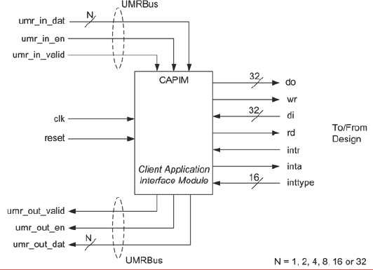
UMRBus, as the new name suggests, is a multi-purpose channel for high-bandwidth commutation with the prototype. It works by placing extra blocks into the design and linking them together via a bus-based protocol which also communicates back to PC-host. There are a number of blocks and other details which we will not cover here, but at the heart of the UMRBus is a simple block called a client application interface module, or CAPIM, a schematic of which is shown in Figure 140.
As we can see in the diagram, a CAPIM appears as a node on a ring communication channel, the UMRBus itself, which carries up to 32 bits of traffic at a time. We can choose a width which best suits the amount of traffic we want to pass. For example, for fast upload of a many megabytes of software image, we might use a wider bus but for setting and reading status registers in the design a 4-bit bus might suffice, saving FPGA resources. Each CAPIM is connected into the design, often using XMRs to save boundary changes, to any point of interest.
Figure 140 : Client application interface module (CAPIM) for UMRBus®
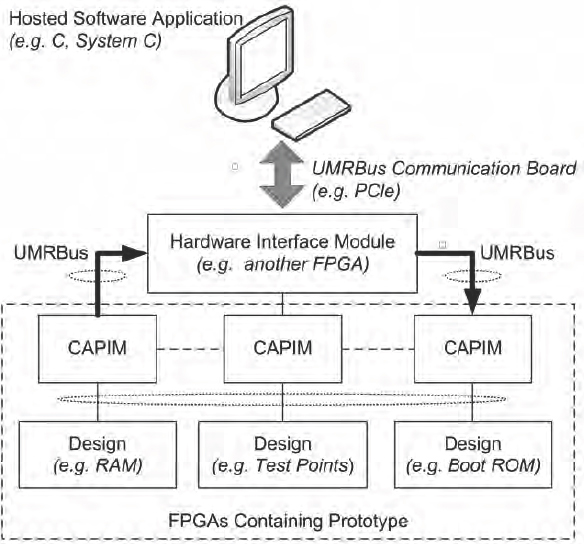
In Figure 141, we can see the use of three CAPIMs on the same UMRBus, each offering access and control of a different part of the prototype. In this example, UMRBus is allowing read and load of a RAM, of some simple registers and test points or to allow reprogramming of the book code in the design.
These functions might all be in the same FPGA or spread across the board across different segments of a UMRBus. Similar in-house proprietary bus-based access systems should also be designed to allow for multi-chip access and cross-triggering.
Figure 141 : UMRBus with three CAPIMs connected into various design blocks
11.6.5. Benefits of a bus-based access system
Some labs have developed their own variations on this bus-based approach and each will have its own details of operation, however, the general aims and benefits are the same as those listed above, so let’s explore how this extra capability can help the FPGA-based prototyping project.
- High speed FPGA configuration: higher bandwidth access to the prototype significantly speeds up the speed at which designs can be downloaded onto the board compared to serial methods typically used. This is especially valuable early in the design cycle when hardware-related design changes most often occur and we are debugging the design’s first runs on the board. The use of a GUI or a command-line interface for configuration and programming benefits greatly from “instant” access and fast configuration, avoiding those irritating delays for a few minutes configurations time.
- An example of a configuration approach which uses a proprietary bus-based interface is the CONFPRO unit from Synopsys which uses the UMRBus protocol to send large amounts of data over USB to an embedded supervisor on the FPGA board which configures the FPGAs in one of their faster parallel modes (see chapter 3) rather than via a JTAG cable.
- High performance memory access: the ability to read and write directly to the memory on the FPGA-based prototype can dramatically reduce bring-up time. On a prototype there can be many megabytes of the FPGA’s internal RAM in use at any time. Memory pre-load and read-back functions can be more easily implemented if an extra bus is placed into the prototype for that purpose rather than trying to employ the SoC’s own CPUs and buses to achieve the same result. We can avoid software rework or scheduling issues involved in having the SoC CPUs simply listen to a host-controlled port and pass data to a RAM.
- Direct access to memory via something like the UMRBus enables us to view memory contents and also rapidly download, upload and compare large quantities of memory content under script control or via TCL commands. A lab library of pre-defined interface objects might be available for connection to our debug bus, such as memory wrappers, which provide a second port into a RAM. This minimizes the need for on-the-spot modeling of many components and speeds access to the system during debug. For example, Synopsys keeps pre-defined IP in the form of a UMRBus-to-SDRAM component, which enables direct access to SDRAM for programming, pre-load and read-back without re-synthesis and/or place & route changes.
- High speed upload of software images: a specific use of the fast-memory access is for loading software images. Since the major use of the prototype may be for enabling a fast and direct platform for the software team, we should enable their normal fast and iterative working methodology. A software image ready for loading into the CPU might be very quickly generated using the normal compile and linking tools. It would then be irritating if it took far longer to load the result into the platform in order to run in. Estimates by colleagues using JTAG-based interfaces tell of 30 minutes to upload a typical software image. This could be cut to considerably less than a minute using a higher-bandwidth interface.
- High-performance data streaming: another use of the faster access into the prototype might be to input data streams from the host at a rate fast enough to fool the SoC design into thinking that it is coming from the real world. Some types of data input might not be suitable for this approach, for example, interactive data or data with a high-rate of delivery such as raw network traffic. Other data, such as imaging or audio data would fit particularly well into this approach. We could, for example, deliver recorded video to the SoC from the host via a bus-based interface to test the software’s capability in a certain video processing task.
- It is a short step from this proprietary data delivery to adopting an industry standard for passing data and even transactions into and out of the prototype. We shall explore this area further in chapter 13.
- Remote configuration and management: with advanced bus-based access, we can remotely access and program the prototype via a host workstation. Board types and configurations could be scanned and their setup requirements automatically detected. Board initialization, configuration and monitoring could then be handled remotely, lightening the burden for a non-expert end-user. For this, it may be necessary to drive the bus-based access from a standard interface port, such as USB. This could be performed via a hardware adaptor which runs the bridge from PCIe (in this case) to the on-board bus access. In the HAPS-60 series of boards, a hardware interface module called CONFPRO connects the PCIe interface on the host workstation to the UMRBus interface on the prototyping system.
In very advanced cases, the bus-based access can become a transport medium for protocol layers but this might be a large investment for most project-based labs, therefore we might expect these types of advanced use modes to be bought in as proven solutions from commercial board and tool vendors.
Once we start to employ the most sophisticated methods for debug and configuration of the system, we might begin to explore other use modes including:
- Direct link to RTL simulator
- Support for transaction-based interface via SCE-MI
- Hybrid system prototyping with virtual platforms We shall explore these in chapter 13.
11.6.6. Custom debug using an embedded CPU
Most of the SoC designs which have embedded processors would also have built-in custom debuggers. These custom debuggers would be used to connect to the processor bus present in the SoC designs, usually to load software programs to be run on the processor, debug the software programs by single stepping or breakpoints and access all the memory space of the processor bus. These custom debuggers will be present inside the design which will be connected to the external world through some dedicated IO ports. Usually a debugging software utility running on a laptop will be connected to these FPGA IO ports using some hardware connected through USB or other IO ports as shown in Figure 142. Using the software utility we can load programs into the program memory, debug the software and access the memory space in the SoC.
Figure 142: Software debugger linked into FPGA-based prototype
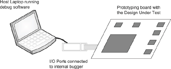
If the design to be prototyped has this debugger, then it can be used to debug the design if it doesn’t work on the board. We should take the dedicated IO ports coming from the inbuilt debugger out of the prototyping board using IO boards or test points. Then the debugging software utility can be connected to these IO ports. After programming the FPGAs, the software utility can be asked to connect to the internal debugger present in the design. Upon successful connection to the internal debugger, we can try to read and write to all the different memory spaces in the processor bus. Then a simple program can be loaded and run on the processor present in the design. Finally the actual software debugging can happen over the real design running on the prototyping board.
11.7. Note: use different techniques during debug
Some might say that on-the-bench debug of any design, not just FPGA-based prototypes, is more intuition that invention. Debug skills certainly are hard to capture in a step-by-step methodology, however, it is a good start to put a range of tools in the hands of experienced engineers. On the bench, it is common to find a combination of these different debug tools in use, such as real-time probing, non real-time signal tracing and customer debuggers.
For example, if a certain peripheral like a TFT display driver in a mobile SoC chip is functioning improperly then we might try to debug the design though the custom debugger first. We could read and write a certain register embedded in the specific peripheral through the customer debugger to check basic access to the hardware. Then we can try to tap onto the internal processor bus through Identify instrumentor and debugger by setting the trigger point as the access to the address corresponding to the register. With the traced signals we can identify whether proper data is read and written into the register. Then we can connect the oscilloscope or logic analyzer on the signals which are connected to the TFT display to check whether the signal are coming appropriately when a certain register is read and written. Of course, all of these steps might be performed in a different order as long as we are successful. With this combined debug approach we can debug most of the problems in the design.
11.8. Other general tips for debug
One of the aims of the FPMM web forum which accompanies this book is to share questions and answers on the subject. The authors fully expect some traffic in the area of bug hunting in the lab and to get us started, here is a miscellaneous list, in no particular order, of some short but typical bug scenarios and their resolutions.
Many thanks to those who have already contributed to this list.
- Divide and conquer: if there are multiple interfaces to the external chipsets, we can test them one by one. Start with the obvious and visible before moving to the obscured and invisible. For example, taking one non-working interface at a time, the interface signals can be probed to see whether the protocol is followed as per the expectations. If they were not followed, we can probe the internal part of the design flow (may be a state machine) which produces those external signals inside the FPGA using Identify or ChipScope, to check whether the flow is proper inside the design. By this way we can test and make sure all the individual interfaces are operating as expected.
- Check external chipsets: the problem may not be in the FPGAs at all. If an external chipset is showing unexpected behavior, then we can try to test the design on the board using synthesizable model of such chipsets implemented temporarily in an FPGA instead. If the synthesizable model is not available for the chipsets then we can consider creating such models themselves or use a close equivalent available as open source. If the functionality is very complex, then at least a model which takes care of the interface part giving some dummy data would be sufficient to test the main design. The open source website www.opencores.org is a good source for synthesizable RTL. Some chipsets have data such as vendor ID or release version hardcoded within them, which can be read through the standard interface. The testing of those external chipsets can be started by reading and verifying such hardcoded data first. This way we can make sure that the interface between the external chipset and the design on the prototyping board works correctly.
- Tweak IO delays: if the input and output delay requirements are not met then the sampling of data inside the FPGA and external chipset will be affected, which can cause data corruption. If this is suspected, then we can try to introduce IODELAY elements present in Xilinx® FPGAs in the data and clock path. IODELAYs are programmable absolute delay elements which can be applied in primary IO paths inside FPGAs. By varying the delay in these blocks, we can make sure that the inputs and outputs are sampled correctly.
- Tweak clock rate: clock rate can be suspected when the design on board is not dead but the operation of the design is not as expected. For example, reading and writing to a memory space might be working but the data read might not be consistent with the written data. If timing issues are suspected (and the PLLs etc. allow running at reduced rates) then we may try to run the system temporarily at reduced clock rate. Often the system can show more signs of life at the reduced clock.
- Understand critical set-up needs: for the design to behave properly, internal blocks might have to be configured in a certain way but some are more critical than others. We should like to be able to rely on documentation sent from the SoC team which highlights the most critical setup. For example, there could be an internal register controlling the software reset of the entire design which might have to be written with a valid value initially to make the design work. As a further example, there could be a mode register which, by default, could be in sleep mode that needs to be written with a valid value to make it active. Similarly some of the external chips might have to be configured in a certain way to make the whole prototyping system work. For example, to make a camera image sensor to send proper images to the FPGA, the internal gain registers in the sensor might have to be configured to a certain non-default value.
- Check built-in security: documentation should record any necessary security or lock cells in the design or external IP. For example, a security code which checks for certain values in an internal ID register, but omitting it means that the prototype will seem alive but unresponsive. As another example, the boot code running the internal process might expect a key bitstream to be present in a flash memory or an external ROM in order to proceed. In such scenarios, it is worth asking again if any such keys are required in the SoC design, just in case documentation has not kept up with the RTL.
- Challenge basic assumptions: one obstacle to debug can be an assumption that the obvious is already correct. We are not asking to check if the power cable is connected (there is a limit) but some basic assumptions should be re-checked, such as little endian-ness and big endian-ness between the buses on FPGAs and any external chipsets or logic analyzers added for prototyping purposes. Another example is to check if any transmit and receive ports in the design should be connected to the external chipsets directly or with crossed wires.
- Terminations: many interface formats such as I2C or PCI or SPI, etc. need the physical lines on the board to be terminated in a certain way. We could check if those lines are terminated as required, if connectors are intermittent or if there are local voltage rails issues preventing correct termination.
- Check IP from the outside-in: while testing the IPs, test the interfaces to the IPs and not the functionality of the IPs themselves. After all, the IPs should have been tested exhaustively by the IP vendor themselves so at least we can initially assume that the IP should work as expected on the FPGA. However, if the IP has been delivered as RTL and not supported for use on FPGA by the vendor/author then we might need to challenge this assumption. IP interfaces can be probed out through logic analyzers or embedded debuggers like Identify or ChipScope.
- Reusing boards allows shortcuts: we could start a debug process from the IPs or design blocks which were known to be working well on the board in a previous project. For example, if the design has a processor and many peripherals we might start with a USB IP which was successfully prototyped earlier. By making sure that the USB IP works fine along with the processor, we can get assurance that at least some software code and the bus through which processor and peripherals communicate is also functioning properly. Then we can debug the new peripherals from a good foundation.
- Test GTX pins first, test protocol second: if the design uses any high speed gigabit transceivers then we can use the integrated bit error ratio tester (IBERT) built into the Xilinx® ChipScope tools. IBERT helps to evaluate and monitor the health of the transceivers prior to testing the real communications through that channel on the board. Only when we are sure about the physical layer should we move on to use our protocol analyzers or bus-traffic mo nitors.
- Use sophisticated analyzers: these analyzers can offer real-time protocol checks, bus performance statistics and can monitor bus latencies. We can also add external bus exercisers to more easily force behavior on the system buses so interference or other de-rating is taking place on the bus inside the prototype. If external equipment is not available, then custom- written synthesizable bus exercisers and bus analyzers might be used. We could consider adding a known, simple checker into the design in order to later use it for checking good bus behavior or forcing traffic.
These are a few of the ideas that Synopsys support staff and end-users have shared over many years of successful prototyping and at time of writing, the authors look forward to hearing many more as the FPMM website goes live.
11.9. Quick turn-around after fixing bugs
Debugging can become an iterative process and given that the time taken to process a large SoC design through synthesis and place & route might be many hours, if we find ourselves wasting a lot of time just waiting for the latest build in order to test a fix, then we are probably doing something wrong.
Here are three approaches we recommended in order to avoid this kind of painful “debug-by-iteration.”
- Stick to a debug plan
- Use incremental tool flows
- Both of the above
A debug plan for a prototype is much like a verification plan for the SoC design as a whole. As a full rerun of the prototype tool chains for large designs might take more than a whole day, we need to have clear objectives for the build, which we should aim to meet before re-running the next build. A debug plan sets out the parts of the design which will be exercised for each build and also a schedule of forthcoming builds. This is particularly useful when multiple copies of the prototype are created and used in parallel. Revision control for each build and documentation of included bug fixes and other changes are also critical. This is all good engineering advice, of course, but a little discipline when chasing bugs, especially when time is short, can sometimes be a rare commodity. With a good debug plan in place and a firm understanding of the aims and content of each build, a regime of daily builds can be very productive.
A day’s turn-around is an extreme example and in some cases it would be much less than that. For example, a bug fix that requires a change to only one FPGA will not require the entire flow to be rerun. The partitioner may work on the design top-down, but for small changes, the previous partition scripts and commands will still be valid. As mentioned in chapter 4, a pre-synthesis partitioning approach helps to decrease runtime in this case because synthesis and place & route take place only on the FPGA that holds the bug fix.
To achieve a faster turn-around on small changes we can use incremental flows and we shall take a closer look at these now.
11.9.1. Incremental synthesis flow
As mentioned in chapter 3, both synthesis and place & route tools have the ability to reuse previous results and only process new or changed parts of the design. Considering synthesis first, the incremental flow in most tools was created to reduce the overall runtime taken to re-synthesize a design when only a small portion of the design is modified. The synthesis will compare parts of the design to the same parts during the previous run. If they are identical then the tools will simply read in the previous results rather than recreate them. The tool then maps any remaining parts of the design into the FPGA elements instead of the entire design, combining the results with those saved from the previous runs of the unchanged parts in order to complete the whole FPGA. This incremental approach can save a great deal of time and takes relatively small effort to set up.
In Synopsys FPGA tools, incremental synthesis is supported by the compile point synthesis flow. In the compile point flow, we manually divide the design into a number of smaller sub-designs or compile points (CPs) that can be processed separately. This does not require any RTL changes but is controlled by small changes in the project and constraint files only, and can even be driven from a GUI.
A CP covers the subtree of the design from that point down although CPs can also be nested as we can see in Figure 143.
Figure 143: possible arrangement for Compile Points during FPGA Synthesis
The design can have any number of compile points, and we do not have to place everything into CPs because the tool makes the top-level a CP by default. Therefore the simplest approach might be to define CPs on all the modules which are frozen or are not expected to change, allowing the tools to simply reuse the previous results for that CP.
Since each CP will be synthesized separately, we must define a separate constraint file for each one which will include many of the same clock and boundary constraints that we would need if the CP block was being assembled in a bottom-up flow, or as a standalone FPGA. Details are of constraints available in the references but the aim is that for a small up-front effort in time budgeting or by limiting our CP boundaries to registered signals, we can dramatically reduce our turn-around time.
The tool needs to be able to spot when the contents of a CP have changed it achieves this by noticing when the CP’s RTL source code logic or its constraints have changed. Changes to some implementation options (such as retiming) will also trigger all CPs to be re-synthesized.
There is no such thing as a free lunch, however, and in the case of incremental flows the downside is that there may be a negative impact on overall device performance and resource usage. This is because cross-boundary optimizations may be arrested at CP boundaries and so some long paths may not be as efficiently mapped as they would have been had the whole design been synthesized top-down. In Synopsys FPGA synthesis this can be mitigated to some degree and the amount of boundary optimizations across the CP boundary can be controlled by setting the CP’s type as either “so ft,” “hard” or “locked.”
Another reason that incremental flows might not yield the highest performance results is that the individual timing constraints for each CP may not be accurate as they rely on estimated timing budgeting or user intervention. Conversely, this might be seen as an advantage since we might purposely choose to tighten or relax the constraints for each CP in order to focus the tool’s effort on more difficult-to-achieve results for certain parts of the design, while relaxing others to save area or runtime.
Readers might be struck by the similarity between CP incremental synthesis and traditional bottom-up synthesis of a design block-by-block. However, the scripting, partitioning and resource management involved in a traditional bottom-up flow is sometimes seen as too much of an investment for a prototyping team. There is also the problem of tracking exactly which files are to be re-synthesized in the new build. In a design of thousands of RTL files, automation is very desirable.
11.9.2. Automation and parallel synthesis
If the workstation upon which the FPGA synthesis is running has multiple processors then the synthesis task can be spread across the available processors, as shown in Figure 144.
With such multiprocessing enabled, multiple CPs can be synthesized simultaneously further reducing the overall runtime of synthesis even for the first run or complete re-builds when all CPs are re-synthesized. By using the automatic CPs and multiprocessing options together, we can reduce the overall runtime of the synthesis during the first time as well as the subsequent incremental iterations.
Figure 144: Automatic compile points and synthesis on multiple CPUs
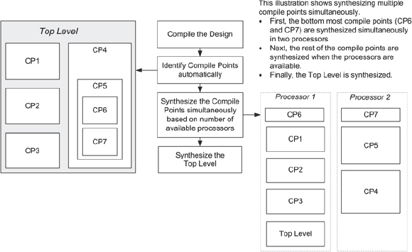
A typical SoC design would need a number of CPs to be defined with individual constraint files in order to achieve a significant reduction in the synthesis runtime. Again, if the up-front investment for an incremental flow is too great or requires too much maintenance (e.g., in scripts) then the flow becomes less attractive. Indeed, defining a large number of CPs and creating constraints files for each may even be seen as too time consuming. To overcome this apparent hurdle, Synopsys FPGA synthesis is able to create and use CPs automatically.
When automatic CPs are used, the tool can analyze a design and identify modules that can be defined as CPs. The CP’s timing constraints can also be automatically budgeted from the top-level constraints. This eliminates the need for us to define a separate constraint file for each defined CP.
This is a relatively new technology and is a useful weapon for trading off runtime against overall performance.
11.9.3. Incremental place & route flow
Incremental flow in place & route can be achieved using design preservation flow in the Xilinx® back-end tool, the flow for which is seen in Figure 145.
Design preservation is one of the hierarchical design flows supported in the Xilinx® back-end tool. In the design preservation flow, the designs are broken into blocks referred to as partitions. Partitions are the building blocks of all the hierarchical design flows supported in the Xilinx® back-end tool. Partitions create boundaries
Figure 145: Design preservation flow in Xilinx® ISE® tools around the hierarchical module instances so that they are isolated from other parts of the design.
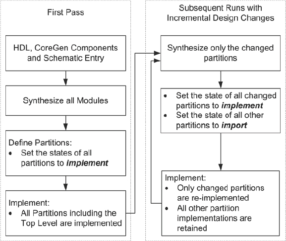
A partition can either be implemented (mapped, placed and routed) or its previous preserved implementation can be retained, depending on the current state of the partition. If a partition’s state is set as “implement,” then the partition will be implemented by force. And if the partition’s state is set as “import,” then the implementation of that partition from the previous preserved implementation will be retained.
When a design with multiple partitions is implemented in the Xilinx® back-end tool for the first time, the state of all the partitions must be set to “implement.” For the subsequent iterations, the state of the partition should be set either to “import” if the partition has not changed or “implement” if it has changed. This way, only the changed modules are re-implemented and the implementations of all the partitions that have not changed are retained. This saves significant time in the implementation of the entire design.
11.9.4. Combined incremental synthesis and P&R flow
Figure 146: Combined synthesis and place & route incremental flow
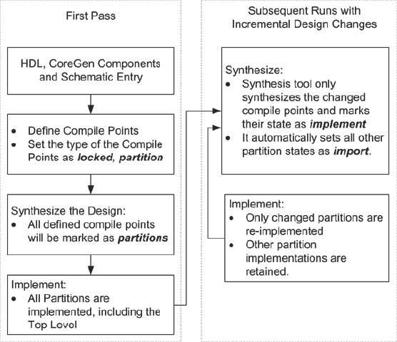
By combining incremental flows for synthesis and for place & route we can gain our maximum runtime reduction. In fact, since place & route runtime is typically much longer than synthesis runtime, setting up incremental synthesis without incremental place & route would not really improve turn-around time that much.
With this in mind, Synopsys FPGA synthesis has been created to interleave its compile point flow automatically with the Xilinx® design preservation flow, as shown in Figure 146. In this integrated flow, the type of CP in the synthesis flow should be set to “locked, partition,” so that it will be marked as a partition during the place & route stage. When the integrated flow is enabled, the Synplify® Premier software automatically writes the states of the partitions as “implement” or ‘import” as appropriate.
By using this integrated flow, as summarized in Figure 146, the overall turnaround time to synthesis, place & route and design can be significantly reduced.
11.10. A bring-up and debug checklist
Table 30: A step-by-step approach to bring-up and debug of the prototype in the lab
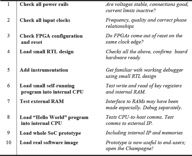
We have covered a lot of ground in this chapter but there will be very many on-the- bench debug scenarios not covered here. Every design and lab setup is different and we can only attempt to cover the more common patterns in the projects that we know.
We hope that there will be a great deal of discussion and “I found this, try that…” experience swapped between prototypers on the FPMM online forum, from which we can all learn to become better debuggers. In the meantime, Table 30 gives a rough checklist of tasks in the lab during bring-up and debug.
11.11. Summary
After giving ourselves confidence that the FPGA board is fully functional and configured correctly and also having checked the implementation and timing reports for common errors, we can consider that functional faults in the operation of the prototype might actually be bugs in the design itself that are becoming visible for the first time.
As we find and correct bugs and move towards a fully functional prototype we are being paid back with interest for all our hard work in getting this far. The prototype has also become an extraordinarily powerful tool for validating the integration of the software with the SoC. Replicating the prototype for use by a wider community of software engineers is relatively quick and simple at this stage.
The authors gratefully acknowledge significant contribution to this chapter from
Ramanan Sanjeevi Krishnan of Synopsys Bangalore