CHAPTER 8 |
PARTITIONING AND |
After following the guidelines in chapter 7, our design will be ready for FPGA, or should we say, ready for one FPGA. What if our design does not fit into a single FPGA? This chapter explains how to partition the FPGA-targeted part of our SoC design between multiple FPGAs. Partitioning can be done either automatically or by using interactive, manual methods and we shall consider both during this chapter. We shall also explain the companion task of reconnecting the signals between the FPGAs on the board to match the functionality of the original non-partitioned design.
8.1. Do we always need to partition across FPGAs?
Many FPGA-based prototypes will use a single FPGA device, either because the design is relatively small or because as prototypers, we have purposely limited the scope of our project to fit in a single FPGA. As explained in chapter 3, FPGA capacity keeps increasing in line with Moore’s law, so one might assume that eventually all prototypes will fit into a single device. However, SoC designs are also getting larger and typically already include multiple CPUs and other large-scale application processors such as video graphics and DSPs, so they will still overflow even the largest FPGA.
As we shall see in chapter 9 on Design-for-Prototyping, an SoC design can be created to pre-empt the partitioning stage of an FPGA-based prototyping project. The RTL is already pre-conditioned for multiple devices and we can consider the SoC design to consist of a number of separate FPGA projects. By planning in advance we can ensure that each significant function of the SoC design is small enough to fit within a single very large FPGA, or otherwise easy to split into two at a boundary with minimal cross-connectivity.
However, some designs do not have such a natural granularity and do not obviously divide into FPGA-sized sections so for the foreseeable future, therefore, we should usually expect to partition the design into more than one FPGA and for some designs this may be a significant challenge. In addition, not only do we need to partition the design but we also need to reconnect the signals across the FPGA boundaries and ensure that the different FPGAs are synchronized in order to work the same as they will have in a single SoC. Let’s look in turn at partitioning, reconnection and design synchronization.
8.1.1. Do we always need EDA partitioning tools?
If we have not designed our SoC expressly for multiple FPGA prototyping, it is unlikely that we will be successful without using EDA tools to either aid or completely automate the partitioning tasks. There are a number of EDA tools that aid in the partitioning effort and greatly simplify it. Generally, these tools take as their inputs the complete design and a system resource description, including the FPGAs, their interconnections, and other significant components in the prototyping system. Some are completely script driven based on a command file, while others are more interactive and graphical. Interactive tools display the design hierarchy and the available resources and allow us to drag-and-drop design elements of sub-trees “into” specific FPGAs. Advanced tools will dynamically show the impact of logic placement on utilization and connectivity.
The following list depicts the advantages of using EDA tools to perform partitioning:
- Global implementation constraints are possible and the tools transparently propagate these constraints to the place & route tools for each FPGA.
- The partitioning tools will optionally insert pin multiplexing and employ logic replication as needed.
- Some partitioning tools are tightly integrated with FPGA synthesis tools allowing resource and timing information to be generated by one and used by the other. This integration further simplifies the partitioning and synthesis processes.
8.2. General partitioning overview
The quality of the partitioning can significantly affect the resulting system size and performance, especially for large and complex SoC designs.
As we saw in chapter 3, there are a number of approaches to partitioning giving us the general choices of partitioning at the RT level before synthesis or at netlist-level after synthesis. In either case, the same general guides for success apply. Partitioning is performed in a number of stages and requires some advance planning. The prime goal of partitioning is to organize blocks of the SoC design into FPGAs in such a way as to balance FPGA utilization and minimize the interconnect resources. Therefore we need to know details of both the size of the different design blocks and also the interconnections between them. We shall consider that in a moment.
8.2.1. Recommended approach to partitioning
Let’s now look at the recommended order in which we should partition the FPGA-ready part of the design. Table 17 summarizes the steps to be taken during an interactive approach. We will consider each in detail in the coming sections and then go on to consider automated partitioning.
Table 17: Major steps in interactive manual partitioning
| Task | Main reasons |
| Describe target resources | Basic requirement for all EDA partitioning tools. (even a manual approach needs pin location list). |
| Estimate area | Avoids overuse of resources during partitioning. |
| Assign SoC top-level IO | Ensures connectivity to external resources. Directs the choice of FPGA IO voltage regions. |
| Assign highly connected blocks | Minimizes inter-FPGA connectivity for large buses. Groups related blocks together for higher speed. |
| Assign largest blocks | Gives early feedback on likely resource balancing. Leaves smaller blocks for filling in gaps. |
| Assign remaining blocks | Allows manageable use of replication and pruning. Allows manageable working at lower levels. |
| Replicate essential resources | Reduces required amount of RTL modification Sync clock and reset elements in each FPGA. |
| Multiplex excessive FPGA interconnect | Frees up FPGA IO for critical paths. May be only way to link all inter-FPGA connections. |
| Assign traces | Assigning inter-FPGA signals fixes pin locations. Every FPGA pin location must be correct. |
| Iterate to improve speed and fit | Initial partition can usually be improved upon. Target speed can often be raised as project matures. |
8.2.2. Describing board resources to the partitioner
In the meantime, we will already have an understanding of the board resources onto which we will need to map the design. We know the size of the FPGAs and have a complete list of the interconnection between them on our board. The partitioning tool will need to have this information presented in the correct format and in the case of the Synopsys Certify® tool, this is called a board description file and is written in Verilog. An excerpt from a board description file is shown in Figure 104, in which we can see clock traces, other traces and an instantiation of a Xilinx® LX760 FPGA.
Figure 104: Excerpt from typical board description for partitioning purposes
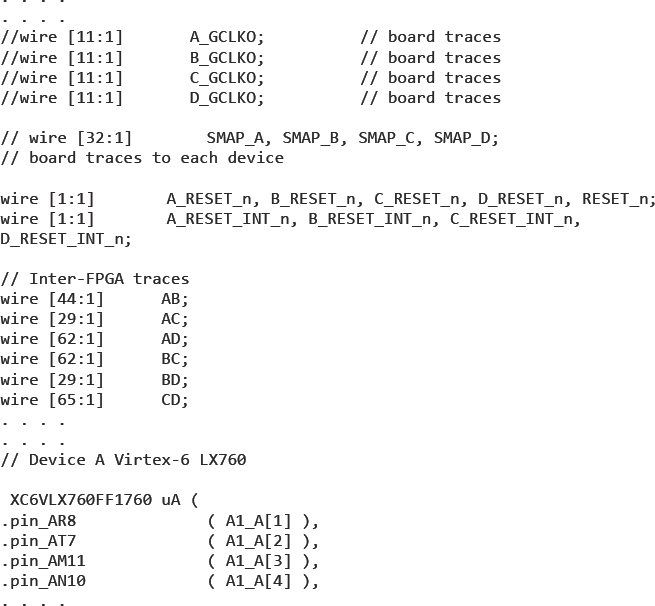
It is not necessary to describe parts of the board that do not affect signal connectivity, so items such as power rails, pull-up resistors, decoupling capacitors or FPGA configuration pins need not be included. It is most important that the connectivity information is absolutely correct and if possible, the Verilog board description should be obtained directly from the original board layout tool. A script can be used to remove unwanted board items and to ensure correlation between the traces on the board and the wires in the Verilog.
Some boards and systems will have methods for generating this board description automatically, reflecting any configurable features on the board or daughter cards connected. For example, some systems have deferred interconnect or switched interconnect, as discussed in chapter 6, and so the board description will need to reflect the actual configuration of the board in our project. We will come back to consider adjustable interconnect in a moment.
Considering the area and interconnect requirements for the design as a logical database, and the board description as a physical database, then our partitioning task becomes a matter of mapping one onto the other and then joining up the pieces. If we take a step-by-step approach to this, we should achieve maximum performance in the shortest time.
8.2.3. Estimate area of each sub-block
In chapter 4 we used FPGA synthesis very early in the project in order to ascertain how many FPGAs we need for our platform. For partitioning, we need to know the size of each block to be partitioned in terms of the FPGA resources. We can do this by analyzing the area report for the first-pass synthesis either manually or by using grep and a small formatting script to create a block-by-block report. However, partitioning tools usually make this process more productive, and provide a number of ways to estimate the block area for LUTs, FFs and specific resources (e.g., RAM, DSP blocks). Most importantly, the tools should also estimate the boundary IO for each block and its connectivity to all other blocks.
Rather than running the full synthesis and mapping to achieve area estimates, we can optionally perform a quick-pass run of the synthesis or a specific estimation tool. For example the runtime vs accuracy trade-offs for the Certify tools are shown in Table 18.
The Certify tool can make these estimates, but more importantly, will also display and use those estimates during the partitioning procedures, as we shall see in a moment.
Table 18: Options for resource estimation in the Certify tool
| Effort Level | Estimation Mode | Description |
| Low | Model based | Uses netlist manipulator to write estimation (.est) file; provides fastest execution time. |
| Medium | Model based | Uses netlist manipulator to write estimation file; improved estimation of registers over low effort but longer execution time. |
| High (default) | Architecture based | Uses FPGA mapper to write estimation file; requires longest execution time. |
The result of estimation will yield values which are general very accurate for IO count, but the area will probably be an over-estimate. However, a good by-product of this over-estimation is that it encourages us to leave more room in our FPGAs. The results of a quick-pass estimation may be displayed in many formats, including text files which can be manipulated and sorted using scripts to extract important information. However the most useful time and place to see the results is during the partitioning, in order to prevent us making poor assignment decisions which cause problems later in the flow.
8.2.4. Assign SoC top-level IO
Certain external resources or connectors on the board may need to connect with specific blocks of the design, for example a RAM daughter card will need to connect with the DDR drivers in the design. This will dictate that the RAM subsystem will need to be partitioned into that FPGA which is connected to the RAM daughter board. Other pins of this kind may be connected to external PHY chips, or to test points or logic analyzer header on the board that will mo nitor certain internal activity.
The location of these kinds of fixed resources should be assigned first, since they are forced upon us anyway. Depending on how flexible your platform may be, it might be possible to alter which FPGA pins connect to these external resources by rearranging the board topology, for example, by placing daughter cards in a different place on the motherboard.
Some teams find that it helps to configure the platform so that one FPGA drives as much of the external SoC IO as possible. This may seem to over-constrain one FPGA but the freedom it gives to assignments in the remaining FPGAs is very helpful.
8.2.4.1. Note: take care over FPGA IO voltage regions
In a typical SoC there will be ports that run at different voltage levels in order to connect to external resources. Consequently in our prototype, we need to configure our FPGA pins so that they can interface at the same voltages. FPGA pins are very flexible and can be set to different voltage standards but they must be configured in banks or regions of the same voltage rather than by individual pin, as we learned in chapter 3
We therefore do not have complete freedom in our FPGA pin placement, so we should assign SoC ports that require specific voltage pins next, although it will still be possible later to move pins within the given voltage region if necessary. For example, in the Virtex®-6 family there are 40 pins in a voltage bank. It is very useful if the partitioning tool gives guidance and feedback on voltage regions and required voltages of the IO while we are partitioning and warns against incorrect IO placements or configuration,
8.2.5. Assign highly connected blocks
We can now start assigning the blocks of the SoC design into specific FPGAs. This first partitioning operation will steer all remaining decisions. As in most projects, it is important to make a good start. We begin with those blocks which share the most interconnect with other blocks, but how do identify those?
It is useful before and during partitioning to compare notes with the SoC back-end engineers who floorplan and layout the IC itself. They will probably be working through a trial implementation of the chip around the same time as the prototype is being created (see chapter 4). Both teams face the same partitioning challenges, especially if there are areas of congestion and high-connectivity in the RTL.
Figure 105: Immediate indication of resource and IO usage in each FPGA
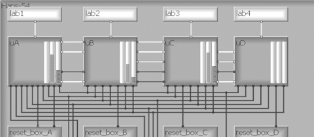
The RTL designers or back-end team may also provide connectivity information, but in many cases we have to ascertain this by inspecting the block-level interconnect information ourselves. This is where some tools can help by displaying or ordering this information for easy inspection, for example, by overlaying the block-level area and interconnect information onto other design views. For example, Figure 105, shows a board view from the Certify partitioning environment where we can see indicators of IO and Logic usage for each FPGA. Interconnect information is also crucial and Figure 106 shows the Certify tool’s display of block-level interconnect data at a particular level of the design hierarchy.
Figure 106: Mutual interconnect between blocks displayed as a matrix
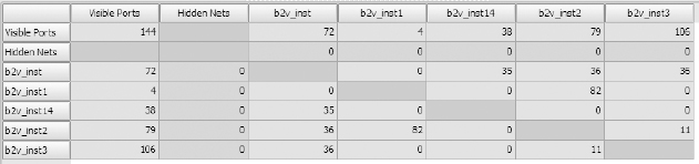
Here we can immediately see that blocks b2v_inst1 and b2v_inst2 share 82 mutual connections but that b2v_inst3 has the most connections (106) to the block’s top-level IO.
The important task when partitioning multiple blocks with large numbers of mutually connected signals is to ensure that these blocks are placed in the same FPGA. If highly connected blocks are placed in different FPGAs then we will need a large number of FPGA IO pins to reconnect them. For example, when using 64 bit and larger buses, it is quite possible that two blocks assigned into different FPGAs can require hundreds of extra FPGA IO. So in our example above, we might try to assign b2v_inst3 first into one FPGA while b2v_inst1 and b2v_ins2 can be assigned together into a different FPGA because they are mutually connected, but share little connectivity with b2v_inst3.
If it is not possible to put highly-interconnected blocks together because they overflow the resources of one FPGA, then we will need to step down a level of hierarchy and look for blocks at the next level which are less connected and extract those to be assigned in a different FPGA. In this way we may still increase the number of required FPGA IO, but by less than would be the case if the higher-level block were assigned elsewhere. If there is no such partition at this lower level then we might go even lower, but specifying partitioning at finer and finer logic granularity makes it more likely that the partition will be affected by design iterations as these finer grains are optimized differently or renamed. If we find ourselves having to go deep into a hierarchy to find a solution then it may be better to go back and restart at the top-level with a different coarse partitioning.
Recommendation: try different starting points and partially complete the assignments to “get a feel” for the fit into the FPGAs and interconnect. If a partitioning effort quickly becomes hard to balance then they are unlikely to complete satisfactorily.
In cases of IO overflow or resource overflow, it is useful to have immediate feedback that this is happening as we proceed through our partitioning tasks. As an example, when block assignments are made to FPGAs in Certify partitioner, we see immediate feedback on IO and resources usage in a number of ways, including the “thermometer” indicators on the FPGAs of the board view, as shown in Figure 105. Here we can see a graphical representation of the four FPGAs on a HAPS® board and in each FPGA, there are three fields showing the proportion of the internal logic resources and the IO pins used in this partition so far. As we assign blocks to each FPGA we will see these thermometers change up, and sometimes down. A glance at this display tells us that the IO and logic usage is well within limits.
8.2.6. Assign largest blocks
Using our estimation for the area of each block, we can assign the rest of the design blocks to FPGA resources, starting with the largest of the blocks. We start with the larger block because this naturally leaves the smaller blocks for later in the partitioning process. Then, with the FPGA resources perhaps becoming over-full (remember 50% to 70% utilization is a good target) we have more freedom in the placement of smaller blocks of finer granularity and lower number of inputs and outputs.
As we partition, we look to balance the resource usage of the FPGAs while keeping the utilization within tolerable limits i.e., less than 70% recommendation. This will help avoid long place & route runtimes and make it easier to reach required timing.
Recommendation: if there is a new block of RTL which is likely to be updated often or to have its instrumentation altered frequently, then keeping utilization low for its FPGA will speed up design iterations for that RTL and save us time in the lab.
As each block is assigned, we may find that the available IO for a given FPGA is exceeded. The remedy for this is to go back and find a different partition or replicate some blocks (see below) or consider the use of time-division multiplexing of signals onto the same IO pin (see also below). At all stages the feedback on current utilization and IO usage will help us to make immediate decisions regarding all the above items.
8.2.6.1. Note: help assigning blocks
Having selected a candidate block for partitioning we might make trial assignments until we find the best solution, however, that is inefficient in a prototype with many FPGAs. We have seen how useful it is to have immediate feedback on our assignment decisions. In fact, it is even more useful to have the feedback before the assignment is made. This allows us to see in advance what would be the effect on IO and resources if a selected block were to be placed in such-and-such FPGAs. This kind of pre-warning is called impact analysis.
In the case of Certify, impact analysis can instantly make the trial assignment to all FPGAs on our behalf and then show us the impact in a graphical view, as shown in Figure 107.
Figure 107: View of impact analysis in Certify tool
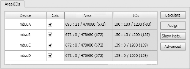
Here we can see that our selected block has an area of 672 logic elements, extracted from a previous resource estimate. If we choose to assign our block to mb.uB, we will increase that FPGA’s area by 672 logic elements (out of a total of 478080) and we will increase the IO count by 137, bringing it to a total of 150. We can also see that if we assign our block to mb.uA, then the area will still increase by the same amount but the IO requirement will fall by 83 pins, presumably because our block connects to some logic already assigned to mb.uA. We can select mb.uA based on this quick analysis and then click assign.
As with all tools driven by an interactive user interface it is good to be able to use scripts and command line once we are familiar with the approach. In the case of Certify’s impact analysis, a set of TCL commands is available to return the requested calculation results on the specified instances for the indicated devices. Results can be displayed on the command line or written to a specified file for analysis.
This semi-automated approach to block assignment leads us to ask why a fully automated partitioning would not be able to perform the same analysis and then act upon the result. We shall look at automated partitioning in a later section.
8.2.7. Assign remaining blocks
After the major hierarchical blocks have been placed, we can simply fill in the gaps with smaller blocks using the same approach. The order is not so important with the smaller blocks and we can be guided by information such as connectivity and resource usage. Some tools also offer on-screen guidance such as “rats-nest” lines of various weights based on required connections which appear to pull the selected block towards the best FPGA to choose.
Having made their key assignments manually, some teams will switch to using automated partitioning at this stage. If this can operate in the same environment as the manual partitioner then that is more efficient. We simply get to a point where we are satisfied that we have controlled our crucial assignments and push a button for the rest to be completed. For example, Certify’s quick partitioning technology (QPT) can be invoked from within the partitioning environment at any time.
8.2.8. Replicate blocks to save IO
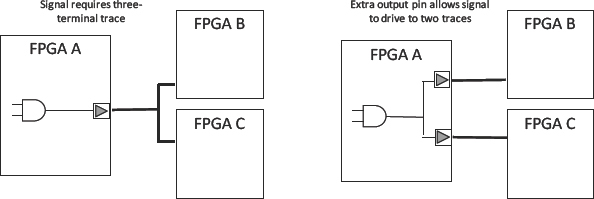
While partitioning a system as large as a complex SoC we are likely at some time to reach a point where a block needs to be in two places at once.
For example, the next block we wish to partition needs to drive a wide bus to two blocks which were previously partitioned into different FPGAs, as shown in Figure 108.
Figure 108: A partitioning task; where to place the next block?
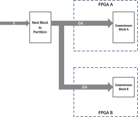
Which FPGA is the right place to put our next block? Either choice will cause thereto be a large number of IO which need to leave the chosen FPGA to connect the bus across to the un-chosen one, as shown in Figure 109.
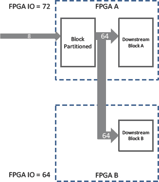
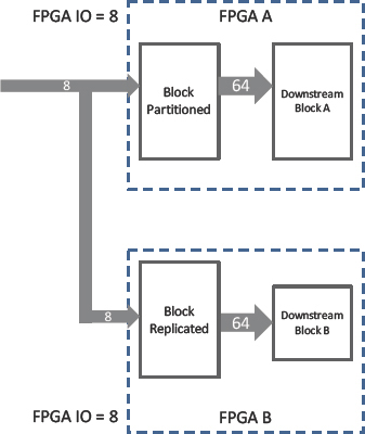
The answer is to put the block into both FPGAs as shown in Figure 110. In this way each downstream block has its own copy of the new block inside its FPGA and so no IO is required except for that which feeds the new block, IO requirement drops from 136 to 16.
Figure 109: Partitioning into either FPGA requires 136 extra IO pins
Our partitioning tool should allow us to make multiple copies of the same block for partitioning into different FPGAs. If not, then it might mean a lot of rewriting of RTL, which may not be practical, even with the use of XMRs and other short cuts.
Partitioning tools will have different ways to achieve this replication but in the case of Certify it is simply a matter of assigning a block to multiple destinations. The multiple assignments will infer additional logic and interconnections, splitting the original blocks fanout into local sub-trees for each FPGA if possible.
Figure 110: Replication and partitioning into both FPGAs requires only 16 extra pins
Because we are making two copies of our new block, the end use of resources will increase, although maybe not as much as first anticipated. Part of the replicated block placed in the second FPGA may not be required to drive logic there while that part of the original is already driving the logic in the first FPGA. Hence parts of the replicant and original will be pruned out during synthesis.
Replication can also be used to reduce the number of IO for a high-fanout block driving multiple FPGAs. The simple, albeit unlikely scenario of an address decoder driving three FPGAs is a good illustration of how we can reduce the number of required on-board traces by using replication to create extra decoders, and then allowing the synthesis to remove unnecessary logic in each FPGA.
Replication is such a helpful trick that, when we are partitioning, or preferably before, we should be on the look-out for replication opportunities to lower the IO requirement.
Replication is also very useful for distributing chip support items such as clock and reset across the FPGAs, as we shall see in section 8.5.
8.2.9. Multiplex excessive FPGA interconnect
As mentioned, large SoCs with wide buses may not partition into a number of FPGAs without overflowing the available IO resources, even when using replication and other techniques. In that case we can resort to using time-division multiplexing of more than one signal onto the same trace.
Multiplexing is a large subject, so in order not to break the flow of our discussion here, we shall defer the detail until section 8.6 below.
Let us assume for the moment that and necessary signal multiplexing has been added and that the interconnect between the FPGAs has been defined. We are now ready to fix the FPGA pin locations. We do this directly by assigning signals to traces.
8.2.10. Assign traces
We have reached the stage in our project where we have partitioned all the SoC into FPGAs, but before running synthesis and place & route, we need to fix the pinout of our FPGAs. All along we have been considering the number of FPGA IO pins as being limited. However, really we should be talking about the connections between those pins on the different FPGAs. The number of traces on the board or the width of cables and routing switches which are able to connect between those FPGA IO pins are the real limitation.
In a well-designed platform, every FPGA IO pin will be connected to something useful and accurately represented in the board description file. Then the partitioning tools will know exactly, and without error, which traces are available and to which FPGA pins they connect. If the board description is accurate then the pin assignments will be accurate as a result.
This section of the chapter is called “Assign traces,” rather than “Assign FPGA pins,” because that is what we are doing. We should not think that we are assigning the signals at the top of each FPGA to a pin on that FPGA, but rather we should think of it as assigning signals to traces so that these propagate to fix all FPGA pins to which the trace runs.
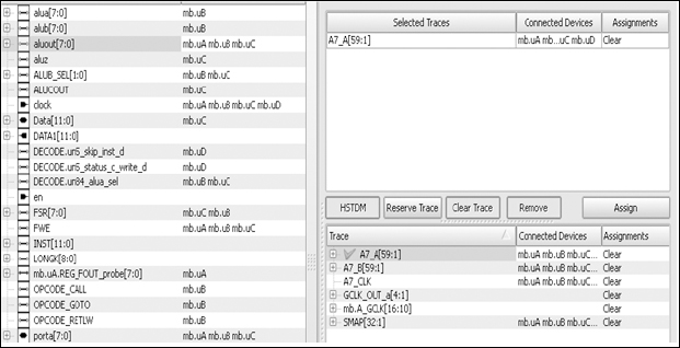
Figure 111: Certify tool’s trace assignment environment
EDA tools such as Certify automate the trace assignment process while keeping track of available traces on the board and permissible voltage regions and allowing automatic signal assignment. The trace assignment environment should help us recognize clock, resets and other critical signals. It should also help us to sort traces by their destinations and fanout and filter suitable candidates for assignment of particular traces. One view of Certify’s trace assignment window is shown in Figure 111, in which we can see the signals which require assignment listed on the left. Here we can see that the user has selected a bus of eight signals called aluout which, as the adjacent list shows, needs to connect to logic which has been partitioned into devices mb.uA, mb.uB and mb.uC. Once a signal or group of signals is selected, at the bottom right there appears a filtered list of candidate traces on the board i.e., those which are available and which connect to at least the required FPGAs (or other board resources should that be the case). We then pick our candidate and confirm the assignment with the relevant button.
The recommended order to assign our signals to traces is as follows:
- Assign clock, reset and other global inputs if any.
- Assign test points or probe outputs to match the on-board connections.
- Assign top-level ports which connect to dedicated resources or connectors.
- Assign rest of inter-device signals, being aware of voltage-level requirements.
In each case, there will probably be more than one candidate trace for any selected signal. We choose from candidate traces in the following preference order:
- Any available trace that has the same end-points as the signal.
- If no trace meets the criteria in 1, then a trace with the same end-points as the signal, plus minimum number of superfluous end-points. Superfluous end-points mean that FPGA pins will be wasted.
- If no trace meets the criteria in 2, then we must split the signal onto two traces using two output pins at the signal’s source FPGA, as seen in Figure 112.
Figure 112: Splitting signal onto two FPGA pins, using two traces to reach destination pins
When there is no trace including at least the end-points required by the signal, then multiple traces between the driving FPGA and each of the receiving FPGAs can be used.
Our EDA tools should be able to split the output onto two FPGA pins automatically without a change to the RTL. This is achieved in Certify by simply assigning the signal to more than one trace. Then the tool increments the pin count on the driving FPGA and the signal is replicated onto the extra trace, or traces.
In general, while following the above recommended preference order there may be multiple equivalent candidate traces to which a signal can be applied and in those cases it is irrelevant which one we choose. This reinforces the notion that for many signals it is not important which FPGA pins we use, as long as they are all connected together on the same trace.
8.2.10.1. Note: automatic trace assignment
Given that the above procedure is fairly methodical, it is relatively simple for EDA tools to make automated assignment following the same rules. In fact, we can take a hybrid approach by making the most important connections manually and allowing the tools to automatically complete the assignments for less critical signals.
Automatic tools will follow a similar order of assignment as we would ourselves. We can minimize the manual assignment steps by giving guidance to the automated tool when it is assigning traces from FPGA to other resources. By naming the signals and the resource pins using the same naming convention, the tools can then recognize, for example, that signal addr1 connects to ram addr1 and its associated trace, rather than any other candidate.
In this way we can methodically step through the trace assignments and guided by our tools, we can quickly assign thousands of FPGA pins without error.
8.2.10.2. Note: trace assignment without EDA tools
The authors are aware of at least one team that has developed its own pin assignment scripts over many projects. These scripts extract the top-level signal names from the log file of dummy FPGA synthesis runs and put them into a simple format that can be imported into the usual desktop spreadsheet applications. The team then uses the spreadsheet to text search the signal names and assigns them to correct FPGA pins. A bespoke board description which includes all the FPGA connections of note is also imported into the spreadsheet. The spreadsheet would then generate pin lists which can be exported and scripted again into the correct UCF format for place & route.
This approach is rare because not only is there the effort of developing and supporting the scripts, spreadsheet and so forth, but it may not also be the core competency of the prototyping team and the best use of its time. In addition, we are introducing another opportunity for error in the project. However, this example does underline the point that we can do FPGA-based prototyping without specialist EDA tools if we are skilled and determined. This might be a “make vs buy” decision that most would avoid, and instead default to using the commercially tried and tested partitioning tools available on the market today.
8.2.11. Iterate partitioning to improve speed and fit
Our first aim, as stated at the start of this chapter, was to organize blocks of the SoC design into FPGAs in such a way as to balance FPGA utilization and minimize the interconnect resources. Once this is achieved, we might want to step back and tweak the partition to improve it, possibly to improve performance.
Recommendation: Take a number of different approaches to partitioning, perhaps with different team members working in parallel, because the starting point can make a big difference to the final outcome The initial block assignment in particular has such a strong impact on later partitioning decisions, so even just having a number of tries at the initial partition may bring some reward.
For example, the major blocks might be split differently and partitioned so that multiplexing is required on a different set of signals, over a different set of traces. The multiplexed paths often become the most critical in the design, so if we can perform multiplexing in a less critical part of the design, then this might raise the overall system performance.
Similarly, replicating larger blocks early in the partitioning, rather than smaller blocks later on, might yield better overall results. If we can make a collection of different coarse partitioning decisions at the start and then explore these as far along the flow as is practical then we can pick the most promising for first completion but perhaps revisiting others when we have learned from our first attempts.
It is often rewarding to discuss partitioning strategies with the SoC back-end layout team as they may have partitioning ideas to share which yield lower routing congestion.
Once we have a finished partition for taking on to the rest of the flow and downloading onto the boards, we can split our efforts and while the FPGA is being brought up and debugged in the lab, we can spare some time in parallel to explore improved results.
During the partitioning task, not only does the design need to be split into individual sub-designs but also consideration must be given to the overall system-level performance of the prototype in the lab. Let us look now at general methods for improving performance in a prototype.
8.2.11.1. Note: explore non-obvious partitions
As we explore different partition ideas, we should try to look beyond the natural functional boundaries within the design. For example, a prime reason why an acceptable partition cannot be found at first might be that a large interconnected block takes up too much FPGA resource. Looking into the next-level hierarchy we find a similar situation, but taking a different view on the blocks might show a datapath structure or a regular channel arrangement which can be split along its length rather than across its block boundaries.
Another alternative partitioning strategy might be to identify all logic within a particular clock domain and then assign it all into the same FPGA. Partitioning tools should have a scripting or graphical method for selecting all logic that is driven by a specific clock. This may also increase performance in a design because the critical path within a domain would avoid traversing an inter-FPGA path. This ideal situation may not arise often in practice, however, owing to other constraints, and in particular, the natural tendency to partition by functionality, rather than by clock domain.
8.3. Automated partitioning
We touched upon impact analysis earlier and considered that it might be possible to automate partitioning based on a similar approach.
Generally, automatic partitioning tools work towards the same prime goals as we would ourselves, namely to minimize IO connectivity between FPGAs and balance resource utilization inside the FPGAs, but they do not have the intelligence to replace an experienced prototyper in finding an optimal solution. What they can do very well, however, is to try very many strategies until something works. An ideal combination may be to use our skill and knowledge to assign an initial set of blocks and then allow the automatic tool to complete the rest.
At the very least we will need to guide the tools. Here are some tasks which should be done manually in order to assist an automatic partitioner:
- Group pins together that need to be connected to an off-FPGA resource (e.g., memory or external interface). If there are no constraints to keep pins together the partitioner may split the pins across all FPGAs. This would be a problem because a typical external resource like a memory is normally connected to only one FPGA.
- Constrain resource usage per device: the automatic partitioner may have a default, but in any case, the available resources (gates, logic, memory) inside an FPGA should be constraint to a maximum of 50 to 70%.
- Populate black boxes or manually assign a resource count so that even the black boxes appear to have some size and then the partitioner will reserve space for that black box. Autopartitioners cannot split black boxes.
- Assign clocks and reset manually: as we would for manual partitioning, special components like the clocks, resets and startup should be replicated into all FPGA and this must usually be done manually (see next section).
- Group blocks together for peak performance: an example here is the manual partitioning of blocks which should stay in one FPGA to get highest performance.
- Allow automatic partitioner to perform multiplexing: the quality of the results will vary from tool to tool, but in those designs which need IO multiplexing, the automated tool may be able to find a solution which allows a lower multiplexing ratio and hence higher system performance.
There are a number of commercially available automated partitioning tools, each with a different approach. However, we must not think of these tools as a pushbutton or optimal solution. The only partitioning tools which come close to this push-button ideal are aimed at quick-pass, low utilization and low performance results, best suited to emulator plat forms. For FPGA-based prototyping, where high-performance is our main aim, this kind of fully automated partitioning is not feasible and it will always be both necessary and beneficial for us humans to stay involved in the process.
8.4. Improving prototype performance
The timing for signals to travel between FPGAs is typically longer than signals that remain inside a given FPGA, therefore inter-FPGA timing is likely to become the limiting factor of the system clock rate, especially in cases where multiplexing is used. We will have a greater impact upon prototype performance if we focus on IO timing and critical inter-FPGA paths. This is done using timing constraints.
SoC top-level constraints apply to the FPGAs down to the level of the individual FFs in their respective clock domains and also between them if cross-domain timing is defined. This is particularly powerful when we can ensure that each FPGA boundary has an IO FF which aligns with a sequential element in the SoC, as we shall see in a moment.
Recommendation: after partitioning, the constraints act upon FPGA synthesis and place & route back-end on each FPGA in isolation so we also need to generate implementation constraints for each FPGA to ensure maximum performance.
We will not give details here of timing constraints in FPGA tools because the references, including the tool vendor’s user guides, are the best source of such information but here are some short notes most relevant to this discussion:
- Synthesis uses estimated timing and maximum delay models for the FPGA.
- Place & route uses exact timing models for maximum timing and statistical estimates for minimum timing.
- The synthesis and place & route tools are timing driven so all paths in the FPGA are constrained, even if only by the global defaults unless explicitly given relaxed timing using false path constraints or other methods to break a timing path.
- Black boxes break a timing path so it is recommended to provide timing information for any black boxes in order to constrain any connected paths.
- FPGA IO pins are considered constrained by the applicable clock constraint.
In general, any FPGA design benefits from plentiful and accurate timing constraints but sometimes designers may not have enough understanding of the final environment or clock domain relationships to create them and this is particularly true for IO constraints. In FPGA-based prototyping we have an advantage in that we have a good understanding of the boundary and external conditions for every FPGA pin. For example, we know the board trace performance, the exact route taken across the board and even the logic in the source FPGA which is driving the signal. These boundary conditions can be automatically translated into the timing constraints necessary for driving both synthesis and place & route for each FPGA in isolation. This process is called time budgeting.
8.4.1. Time budgeting at sequential boundaries
We can improve the timing of any inter-FPGA path by ensuring that there are FFs at the FPGA pins on the path. This is because the clock-to-output delay on the source FPGA output pin and the set-up time on the destination FPGA input pin(s) are minimized.
As we saw in chapter 3, every FPGA IO pad has multiple embedded FFs and these are available to us “free-of-charge,” so why not use them? If we can use these IO FFs in our prototype then they will also provide an additional benefit that the SoC top-level constraints will apply by default to all FFs.
FPGA-to-FPGA timing using the above ideal mapping is constrained by the top-level constraints which automatically propagate to the FFs at each end of any path, internal or external, unless overridden locally. Therefore, the constraints applying to SoC FFs mapped into IO FF are simplified and the FPGAs can be more easily constrained in isolation. This helps in our EDA tool flow because top-level constraints will be automatically reapplied to the FPGAs during each design iteration.
If the partition or the SoC design does not provide FFs which can be placed readily in the FPGA’s IO FF, then is it feasible to add these manually or via scripted netlist editing? The addition of extra FFs into an SoC path just so that they can be mapped into IO FFs would, of course, introduce pipeline delays into that path, altering its system-level scheduling. For prototyping purposes we cannot arbitrarily add such extra FFs, tempting as this may be for the improved performance, without checking with the original designers and probably adding compensating FFs elsewhere in order to maintain scheduling across the design.
Recommendation: addition of pipeline FFs can improve prototype performance but must be acceptable to the SoC design team and a re-run of system-level simulation is recommended.
It is therefore preferable to have FFs at every SoC block boundary and to only partition at those block boundaries and these are indeed recommendations of a possible project-wide Design-for-Prototyping approach that we explore further in chapter 9.
8.4.2. Time budgeting at combinatorial boundaries
If the insertion of FFs at FPGA boundaries or movement of the existing FFs to those boundaries is not possible for all signals, then careful timing constraints for the combinatorial paths across the FPGA boundaries must take place. In this case, we need to evaluate and divide the timing budget between the FPGAs based on the complexity of each section of the path.
Considering a typical path origination in an internal FF on one FPGA that ends at an internal FF in a different FPGA, we would need to break the applicable FF-to-FF constraint, perhaps derived from the top-level SoC constraints mentioned above. Since only the total path is controlled by the system-level constraint we need to determine how much of that constraint should be applied to the two parts of the path as mapped into the two FPGAs. The resulting IO constraints would then be passed on to subsequent synthesis and place & route for each FPGA.
This is especially important for designs which require highest performance because the presence or absence of accurate IO constraints will drive quite different results in the place & route tool. By default, both synthesis and place & route working on the isolated FPGA after partitioning will assume that a whole period of the respective clock is available for propagating the signal to/from the IO pin to/from the internal FF. However, this assumption will almost certainly not be correct.
For example, if the signal has come from an internal FF in another FPGA, then the data will have to traverse that FPGA’s internal routing, its output pad delay plus the board trace delay before arriving at the receiving FPGA’s pin. The receiving FF’s clock will probably have been generated internally in the receiving FPGA. We can therefore see that considerably less than the whole clock period would be available for propagating the signal through the input pad to the receiving FF in order to meet its set-up timing requirement. Relying on the default is risky and so we need to give better IO constraints at combinatorial boundaries, but what should those values be?
It is worth noting that a semi-manual approach could be taken: extracting delay information from a first-pass FPGA timing analysis and then using a spreadsheet to calculate more accurate IO constraints. However, creating IO constraints for many hundreds or even thousands of signals at combinatorial partition boundaries would be a long and potentially error-prone approach. It would also need to be repeated for every design iteration.
Another workaround would be to apply a default of a half-clock cycle of the receiving FF’s clock and this coarse value may be adequate for a low performance target.
Figure 113: Time budgeting at combinatorial partition boundaries
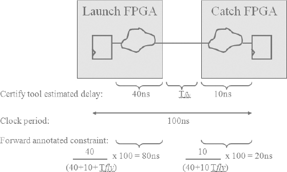
The good news is that automatic and accurate timing budgeting at combinatorial partition boundaries is possible. The Certify tool, for example, uses a simple algorithm to budget IO constraints based on the slack of the total FF to FF. The synthesis is run in a quick-pass mode to estimate the timing of a path accounting for IO pad delays and even the trace delay. Multiple FPGA boundaries and different clock domains in a path are also incorporated in the timing calculation. The result is a slack value for every multi-FPGA path and we can see the proportion of the path delay shared between the FPGAs. An example of this is shown in Figure 113 with exaggerated numbers just to make the sums easy. We see that the timing budgeting synthesis has estimated that 40ns of the total clock constraint of 100ns is spent traversing the first FPGA and 10ns is spent in the second FPGA. There is also a time allowance for the “flight time” on the trace between the FPGAs.
The total permitted path delay (usually the clock period) is budgeted between the devices in proportion to each FPGA’s share of the total path delay. Therefore if either the launching or catching FPGA has a larger share of the total path delay, then the place & route for that FPGA will also have received a more relaxed IO timing constraint i.e., the path is given more time. This is a relatively simple process for an EDA tool to perform but can only be done if the tool has top-down knowledge of the whole path.
This all assumes an ideal clock relationship between the source and destination FPGAs on our boards and we may need to take extra steps to ensure that this is really so, as we shall see in section 8.5.1.
8.5. Design synchronization across multiple FPGAs
Our SoC design started as a single chip and will end up the same way in silicon but for now, it is spread over a number of chips and the contiguity of the design suffers as a result. We have discussed some of these ways we can compensate for the on-chip/off-chip boundary to improve performance and later we shall discuss multiplexing of signals.
There are three particular aspects of having our design spread over multiple chips that we need to concentrate upon. These are the clocks, the reset and the start-up conditions. For complete fidelity between the prototype and the final SoC, then the clock, reset and start-up should behave as if the hard inter-FPGA boundaries did not exist. Let’s consider each of these in turn.
8.5.1. Multi-FPGA clock synchronization
We saw in chapter 5 how the FPGA platform can be created with clock distribution networks, delay-matched traces and PLLs in order to be as flexible as possible in implementing SoC clocks. Now is the time to make use of those features.
There are two potential problems that occur when synthesizing a clock network on a multi-FPGA design:
- Clock skew and uncertainty: a common design methodology uses the board’s PLLs to generate the required clocks and distribute them as primary inputs to each FPGA. The on-board traces and buffers can introduce some uncertainty and clock skew between related clocks due to the different paths taken to arrive at the FPGAs. If ignored, this skew can cause hold-time violations on short paths between these related clocks.
- The back-end place & route tools can typically resolve hold-time violations within the FPGA but cannot currently import skew and uncertainty information that is forward-annotated from synthesis. To address this problem, the FPGAs own PLLs (part of the MCMMs in a Virtex®-6 FPGA) can be used for clock generation in combination with, or instead of the board’s PLLs,. The back-end tools understand the skew and uncertainty of an MCMM and can account for them during layout. However this use of distributed MCMMs can introduce the second of our potential problems mentioned above.
- Clock synchronization: When related clocks are regenerated locally on each FPGA there is a potential clock-synchronization problem that does affect the original SoC design, where clocks are generated and distrusted from a common source. The problem becomes particularly apparent when multiple copies of a divide-by-N clock are derived from a base clock but are not in sync because of reset or initial conditions and just unlucky environmental glitches.
Partitioned designs have their clock networks distributed across the FPGAs and other clock components on the board. Spanning a large number of different clocks across all FPGAs can be made easier by successful clock-gate conversion (see chapter 7), reducing the number and complexity of the clocks. However, there will still be a number of clock drivers which need to be replicated in multiple FPGAs. It is important that these replicated clocks remain in sync and that any divided clocks are generated on the correct edge of the master clock. This is dependent upon the application of reset on the same clock edge at each FPGA as we shall describe in the next section.
We therefore have a generic approach to clock distribution as shown in Figure 114, in which we see the source clock generated on a board while the local MMCMs are used in each FPGA to resynchronize and then redistribute the clocks via the BUFG global buffers. In many cases this small FPGA-clock tree will need to be inserted into the design manually. The latest partitioning tools are introducing features which automatically insert common clocking circuitry into each FPGA.
Figure 114: Clock distribution across FPGAs
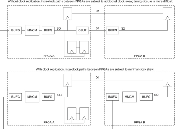
Our earlier recommendation to design the SoC with all clock management in a top-level block will really help now. We only need to make changes at that one top-level block and then use replication to partition the same structure into each FPGA. Even if the clocking in the SoC RTL is distributed throughout the design then replication will help us restrict the changes to fewer RTL files than might otherwise be necessary.
Replication of clock buffers might be avoided if we use a technique discussed in section 8.2.11.1 above for partitioning by clock domain. Success of this approach will depend on relative fanout of the different clocks and the number of paths between domains.
Whatever the partitioning strategy, each FPGA is a discrete entity and for clock synchronization, each must have its own clock generation rather than relying on clocks arriving from a generator in another FPGA. Therefore a clock generator must be instantiated in each FPGA even if only a small part of the SoC design is partitioned there.
Let’s look a little more closely at the clock generator and how it helps us during prototyping. The MMCM’s PLL has a minimum frequency at which it can lock and so the input clock to the FPGA must drive at least at that rate. Virtex®-6 MCMMs have a minimum lock frequency of 10MHz, compared to 30MHz or higher for previous technologies, which makes them particularly useful for our purposes. They are able to generate much slower clocks than they can accept as inputs. Our task is therefore to assemble a clock tree across the prototype where we maintain a higher frequency outside of the FPGAs and then divide internally while keeping the internal clocks in sync.
We achieve this as follows:
- If the SoC has clock generator at the top-level as recommended then
- Create a clock generator block in RTL to replace the equivalent part of the SoC generator. We use a global base clock to drive MCMMs which generate slower derivatives via its divide-by-n outputs.
- Select any one global system clock generated on board; its frequency must be above the minimum MMCM lock frequency.
- Drive the input to the new RTL clock tree with the global clock.
- In the new clock generator RTL, create a tree of MMCM and BUFG instantiations to create all necessary sub-clocks.
- During partitioning, replicate the MMCM and BUFGs into each FPGA as required to drive logic assigned there.
- During trace assignment, the global clock must be assigned to the global clock inputs for the FPGA.
- If clock gating and generation is more distributed then we may need to instantiate BUFG and MMCM components directly into different RTL files, but we should always be on the lookout for how replication can make this process easier.
For multi-board prototypes, we may need an extra level of hierarchy in the clock tree. We should use the on-board PLLs to drive the master clock to each board and resynchronize using PLLs at each board, using the board’s local PLL output to drive each FPGA locally as described above. Skew between boards is avoided by using PLLs and matched-delay clock traces and cables as described in section 5.3.1.
Because multiple PLLs and MCMMs may be used, the local slow clocks must be synchronized to the global clock. This is achieved by using the base clock as the feedback clock input at each MMCM.
We might ask why we do not generate all clocks using the on-board global clock resources. After all, we might have placed specialist PLL devices on the board with, for example, even lower minimum lock frequencies. The issue to be aware of here is that, depending upon the board, there may be some skew between the arrival times of the clocks at each FPGA, especially for less sophisticated boards not specifically designed and laid out for this purpose. This effect will be magnified in a larger system and could lead to issues of hold-time violations on signals passing between FPGAs.
8.5.2. Multi-FPGA reset synchronization
There will be “global” synchronous resets in the SoC which will fan out to very many sequential elements in the design and assert or release each of them synchronously, on the same clock edge. As those sequential elements are partitioned across multiple FPGAs it is obviously critical to ensure that each still receives reset in the same way, and at the same clock edge. This is not a trivial problem but distributing a reset signal across several FPGAs in a high-speed design can be achieved with some additional lines of code in the RTL design and a partitioning tool that allows easy replication of logic.
The enabling factor in this approach is that it is unlikely that the global reset needs to be asserted or released at a specific clock edge, as long as it is the SAME clock edge for every FPGA. Therefore, we can add as many pipeline stages into the reset signal path as we need and we shall use that to our advantage in a moment.
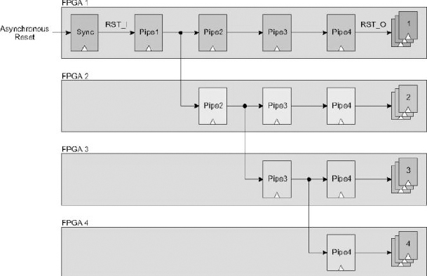
Another factor to consider is that the number of board traces which connect to every FPGA is often limited so the good news is that we do not need any for routing global resets. Instead we create a reset tree structure which routes through the FPGAs themselves and then uses ordinary point-to-point traces between the FPGAs. Considering the design example in Figure 115 in which a pipelined reset drives sequential elements in four different FPGAs, it is clear that the elements in FPGA 4 will receive the reset long after those in FPGA 1.
Figure 115: Pipelined synchronous reset driving elements in 4 FPGAs
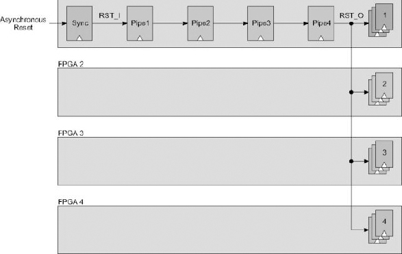
Notice also that the input could be an asynchronous reset, so the first stage acts as a synchronizer (with double clocking if necessary for avoiding metastability issues). Routing through the FPGAs in this way is not acceptable except for very low clock rates, so to overcome this we will replicate part of the pipeline in each of the FPGAs as shown in Figure 117.
Readers using Certify will find further instructions on the correct order for replication in the apnote listed in this book’s references.
The first stage is not replicated because the synchronization of the incoming reset signal has to be done in only one place. There is still a possibility that the pipeline stage in each FPGA would introduce delay because if there is one FF in each stage, then it might be placed near the input pad, the output pad or anywhere in between; this might also be different in each FPGA. The answer is to use three FFs for each pipeline stage, as shown in Figure 116.
Figure 117: Tree pipeline created by logic replication
This allows the first and third FF to be placed in an IO FF at the FPGA’s edge. Then there is a whole clock period for the reset to propagate to the internal FF and on to the output FF, greatly relaxing the timing constraint on place & route. Once again, these pipe stages only introduce an insignificant delay compared to the effect of the global reset signal it self.
Figure 116: A three-FF pipeline stage gives more freedom to place & route
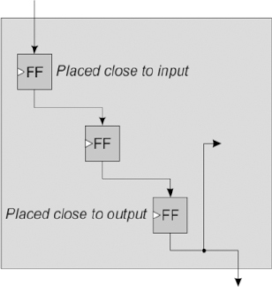
Note: the synthesis might try to map the pipeline FFs into a single shift register LUT (SRL) feature in the FPGA, which would defeat the object of the exercise so the relevant synthesis directive may be required to control the FF mapping. In the case of Synopsys FPGA synthesis, this would be syn_srlstyle and for good measure syn_useioff would be used to force the two FFs into the IO FF blocks, although that is the default.
8.5.3. Multi FPGA start-up synchronization
Using the above technique we can ensure that all FPGAs emerge from start-up simultaneously. But this is of little use if the clocks within a given FPGA are not running correctly at that time. We must also ensure that all FPGA primary clocks are running before reset is released. This is important because, owing to analog effects, not all clock generation modules (MMCMs, PLLs) may be locked and ready at the same time. We must therefore build in a reset condition tree. This can be accomplished by adding a small circuit like the one shown in Figure 118 which would be distributed across the FPGAs.
Here we see a NAND function in each FPGA to gate the LOCKED signals from only those MCMMs which are active in our design. This would be a combinatorial function or otherwise registered only by a free-running clock that is independent of the MMCM’s outputs.
Figure 118: Example reset condition tree
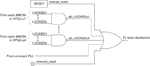
Each FPGA then feeds its combined all_ LOCKED signal to the master FPGA in which it is ORed to drive the reset distribution tree described in the previous section. The locked signals of any on-board PLLs used in this prototype must also be gated into the master reset and there may other conditions not related to clocks which also have to be true before reset can be released, for example, a signal that external instrumentation is ready and, of course, user’s “push-button” reset should also be included. Our example shows that these are all active high but of course the reset gate can handle any combination. The whole tree would be written in RTL which is added into the FPGA’s version of the chip support block at the top level and we can use replication to simplify its partitioning.
The global reset is only released when all system-wide ready conditions are satisfied. The reset will also then release all clock dividers in the various FPGAs on the same clock edge so that all divide-by-n clocks will be in sync across all FPGAs.
8.6. More about multiplexing
The partitioning is done. The resource utilization of all FPGAs is well balanced and within the suggested range. Furthermore, the design IOs per FPGA are minimized but after such good work, there is still a chance that there are not enough FPGA pins available to connect all design IOs, or to be more accurate, there are not enough onboard traces between some of the FPGAs. As mentioned in section 8.2.9 above, the solution is to multiplex design signals between FPGAs in question. Multiplexing means that multiple compatible design signals are assembled and serialized through the same board trace and then de-multiplexed at the receiving FPGA. We shall now go into more detail on how this is done and also compare different multiplexing schemes. We shall also explain the criteria for selecting compatible signals for multiplexing and give guidance on timing constraints.
8.6.1. What do we need for inter-FPGA multiplexing?
To multiplex signals between FPGAs we need a number of elements including a multiplexer (mux), demultiplexer (dmux), clock source and a method for keeping all of these mutually synchronous. All of these elements are seen in the in Figure 119 (see next section for full explanation).
If we have freedom to alter our RTL then theoretically, these elements could be manually added at each FPGA boundary. We would need to add the multiplexing elements after partitioning or add the elements into the RTL from the start, therefore pre-supposing the locations for partition boundaries. In both cases, the rest of the SoC team might see this as stepping too far away from the original SoC RTL and introducing too many opportunities for error.
Most teams would not contemplate such widespread changes to the SoC RTL and instead they rely on automated ways to add the multiplexing, either by scripted direct editing of the post-synthesis netlists or by inference during synthesis, based on direction given by the partitioning process. We shall explain more about this in a moment.
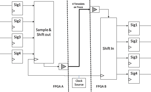
Figure 119: Basic time-division multiplexing of inter-FPGA signals
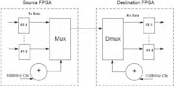
Whatever the method for introducing the muxing, the basic requirement of the scheme is to transfer IO data values from one FPGA to another within one design clock. To achieve this, the serial transfer clock (also named multiplexing clock or fast clock) must sample those data values faster than the design clock to guarantee that all the data is available in the receiving FPGA before the next active design clock edge.
As an example, let’s assume that we have four IO data values to transfer between two FPGAs which are multiplexed on a single on-board connection i.e., a mux ratio of 4:1. If this part of the design is running at 20MHz then, to transfer the four design IOs within a design clock cycle, we need a transfer clock which is at least four times faster than the design clock. Therefore the transfer clock must be 80MHz at minimum. In practice it needs to more than four times faster for a multiplexing of 4:1 because we need to ensure that we meet the setup and hold times between the data arriving on the transfer clock and then being latched into the downstream logic on the design clock.
In most of the cases where multiplexing is used, it decreases the overall speed of the design and is often the governing factor on overall system speed. The serial transfer speed is limited by the maximum speed through the FPGA IOs and the flight time through the on-board traces. Therefore, with these physical limits the multiplexing scheme needs to be optimized to allow the prototype to be run at maximum speed.
Multiplexing is typically supported by partitioning tools which insert the mux and dmux elements and populate them with suitable signals. For example, in the Certify tool there are two different types of scheme called certify pin multiplier (CPM) or high speed time domain multiplexing (HSTDM).
Based on the relationship of the transfer clock and design clock, we can differentiate between two types of multiplexing. Asynchronous multiplexing, where the transfer clock has no phase relation to the design clock, and synchronous multiplexing, where the transfer clock is phase aligned to the design clock, and probably even derived from it.
8.7. Multiplexing schemes
The partitioning tools insert multiplexing based on built-in proprietary multiplexing IP elements. We normally do not know, or probably need to know, every detail of these elements but we shall explore some typical implementations in the rest of this section. At the end of the section a comparison of the different schemes is shown.
8.7.1. Schemes based on multiplexer
The simplest scheme is a mux in the sending FPGA and a dmux on the receiving FPGA, much as we saw in Figure 119 but with the source FFs omitted. In the source FPGA there is a 100MHz transfer clock which drives a small two-bit counter which cycles through the select values for the mux. Every 10ns a fresh data value starts to traverse the mux, over the board trace and into the dmux in time to be clocked into the correct destination FF. Meanwhile, the dmux is switched in sync with the mux as both are driven by a common clock, or more likely two locally generated clocks which are synchronized as mentioned in section 8.5.3 above.
On each riding edge of the transfer clock, new data ripples through to the mux output and propagates across the trace from the source FPGA to the destination FPGA in time for the receiving register to capture it. This is an extra FF driven by the transfer clock rather than the design FF that would have captured the signal if no multiplexing scheme had been in place.
To use this simple scheme, we need to select candidate signals that will propagate across the mux and dmux in order to meet the set-up timing requirement of the receiving FF. If the timing of the direct inter-FPGA (i.e., non-multiplexed) path was already difficult for the receiving FF to meet, then this is not a good candidate for multiplexing. In normal usage, we would select signals with a good positive slack and these can be estimated after a trial non-partitioned synthesis.
Best candidate IOs for this simplest kind of multiplexing scheme are those directly driven by a FF, which normally could map into IO FFs in the FPGA if there were enough pins available. These would have the maximum proportion of the clock period available to propagate to the destination, assuming that the transfer clock is in synchronization with the design clock driving those FFs. Using IO FFs, the timing of inter-FPGA connections is more predictable and generally faster. Therefore a multiplexing scheme should use IO FFs if possible and we should use synthesis attributes to ensure that a boundary FF is mapped into an IO FF if physically possible.
Another multiplexing scheme, which is very similar to the one described above, has additional sampling FFs in the source FPGA driven by the transfer clock exactly as seen in Figure 119. Now the whole mux-dmux arrangement is in sync with the transfer clock and it is easier to guarantee timing. In fact we need not even have a transfer clock that is synchronous with the design clock but double-clocking synchronizers may be necessary to avoid metastability issues.
8.7.2. Note: qualification criteria for multiplexing nets
There are different types of signal in the SoC design, on different kinds of FPGA interconnections. Some types are suitable for multiplexing and other types should not be multiplexed. Table 19 summarizes these different types and their suitability for multiplexing.
To get the highest performance in case of multiplexing the user should carefully select the FPGA interconnection which should be multiplexed. For designs with different design clocks the user should multiplex signals coming from a low-speed clock with a higher ratio than signals from a high-speed clock. This keeps the performance of the design high.
Table 19: Which nets are suitable candidates for multiplexing?
| Net topology | Suitable? | Notes |
| Nets starting and ending at sequential element. | YES | If possible put sequential element in IO FF. |
| Nets starting at combinational element and but ending on sequential element. | YES | It could be difficult to meet the timing between design clock and multiplexing clock. |
| Nets between FPGAs which are also top-level design IO ports. | NO | Connected external hardware cannot perform dmux. |
| Nets starting and ending at sequential element but in different clock domains. | NO | This has unpredictable behavior owing to setup and hold. |
| Nets starting and ending at sequential elements but feeding through* intermediate FPGA. | NO/(YES) | In theory it’s possible to multiplex such a net but it decreases the design performance and timing is hard to estimate. |
| Nets crucial to the clocking, reset, start-up and synchronization of the prototype. | NO | Crucial nets should be assigned to traces before mux population is decided. |
* feed-through means that there is a path through an FPGA without sequential elements.
8.7.3. Schemes based on shift-registers
Another solution is based on shift-registers, as seen in Figure 120. Here the data from the design is loaded in parallel into the shift-register on the rising edge of the transfer clock and shifted out with the same clock.
In the receiving FPGA, a shift-register samples the incoming data on the transfer clock and provides the data in parallel to the design. The first sample (in this case sig 4) is available at the shift register output from the sample clock edge but an extra edge of the transfer clock may be necessary in some versions of this scheme in order to latch in the data after it has been fully shifted into the destination registers for finally clocking into the design FFs in the destination FPGA. Once again, the sending and receiving shifters need to start up and then remain in sync.
This type of scheme is well suited for boards with longer than average flight time on the inter-FPGA traces because there is no extra combinatorial delay in the path and we obtain maximum use of the transfer clock period. In particular, it is not acceptable to have new data being sampled onto the trace if the previous sample has not yet been clocked into the receiving logic. In some lab situations we can get lucky, but in others, the transmission line characteristic of the trace or a slight discontinuity in a connection can make the transfer unreliable. Therefore we have
Figure 120: Basic time-division multiplexing based on shift registers an upper physical limit on transfer clock speed and if we hit that then the only way to increase multiplexing ratio further is by reducing the overall system speed. Having done so, then even when using mux ratios of 10:1 or higher, we just have to operate the prototype at a lower clock rate.
8.7.4. Worked example of multiplexing
It is important to understand mux timing so here is a worked example of a multiplexing solution that uses a mux followed by a sampling FF. Considering the Figure 121, in FPGA A we have a design with some flip-flops which we call FFs followed in this example by some combinatorial design logic (in some other examples it might also be possible that there are only design flip-flops). The values are fed to the send stage which contains a multiplexer which selects each design signal in turn and an output FF, which we shall call FFMO. FFMO could be placed into an IO FF of FPGA A in order to improve the output timing as mentioned above.
Figure 121: Example time-division multiplexing based on sample register
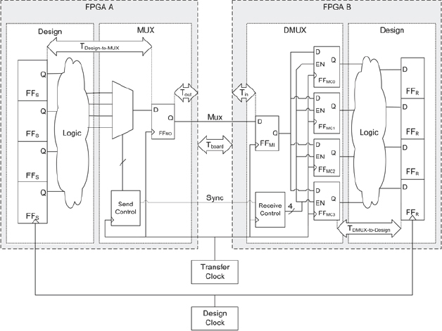
Between the two FPGAs we use a single-ended connection for the multiplexed signals (shown as mux on our diagram). As mentioned above, to guarantee signal integrity we must ensure that a multiplexed sample is received and latched into the destination FF within one transfer clock cycle between the sending FFMO and the receiving FF, which we shall call FFMI.
As the multiplexed samples are clocked one by one into FFMI in FPGA B, they are stored in a bank of capture FFs, which we call FFMC. These capture FFs ensure that the samples are all stable before the next clock edge of the design clock. Our example also shows some combinatorial design logic in the receive side (but again, this might only be design FFs). The aim is to show that TDM can be used on a wide variety of candidate signals.
Now let’s see how we can calculate the maximum transfer frequency and the ratio between transfer clock and design clock.
Our constraint is to transfer a data value within on period of the transfer clock cycle between FFMO and FFMI. The delays on the path are as follows:
- The delay through the output buffer of FPGA A (Tout)
- The delay on board (Tboard)
- The delay of the input buffer at FPGA B (Tin)
The maximum delay on the multiplexing connection is therefore:
TMUXmax = Tout + Tboard + Tin
If we assume typical values of Tout = 5ns, Tboard = 2ns and Tin = 1 ns we get a maximum delay of:
TMUXmax = 5ns + 2ns + 1ns = 8ns
This sets the upper limit on transfer clock frequency of:
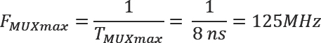
That’s the theoretical rate that signals can pass between the FPGAs, but we should also respect that we are using single-ended signaling and that there can be some clock uncertainty, or jitter, between the FPGAs and we should also give some room for tolerances. Therefore, based on our experiences, we should add Ttolerance = 1 - 2ns to provide some safety margin, depending how confident we are in the quality of the clock distribution on our boards. For our example let’s assume that Ttolerance= 2ns. This results in the following calculation:
TMUXmax = Tout +Tboard + Tin + Ttolerance
If we assume the same values as above for the other delays we get:
TMUXmax =5ns + 2ns + 1ns + 2ns = 10ns
and a maximum transfer clock frequency of:
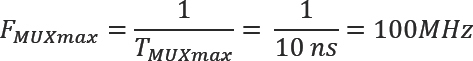
The maximum clock frequency of 100MHz (or period of 10ns) must be given as a constraint on the transfer clock during FPGA synthesis and place & route.
Let’s now consider a little more closely how the mux and dmux components are working in order to calculate the ratio between transfer clock and design clock. We have to consider two possible use cases. The first case is that that the transfer clock and the design clock are mutually synchronous i.e., they are derived from one clock source and they are phase aligned. The second case is that the transfer clock and the design clock are asynchronous, in which case, we don’t know on which transfer clock cycle the transfer of the data values starts and we have to set the right constraints to make sure that it works.
Starting with the synchronous case, we see from the block diagram that there are some transfer clock cycles required to bring the data from the sending design FFS through the multiplexing registers FFMO, FFMI, FFMC to the receiving design register FFR.
In addition, even though the two clocks are synchronous, we have to respect the delays between the design clock and the transfer clock on the sending and receiving side. These delays are marked in the block diagram with Tdesign-to-mux for the sending side and Tdmux-to-design for the receiving side. For the following calculation of the clock ratios we assume that these delays have a constant value and we have to give these assumptions as constraints to synthesis and place & route. For our example here we shall assume that these delays are a maximum of one transfer clock cycle, which is extreme, and a maximum of 10ns.
Table 20 shows how the design signals are transferred through the multiplexing based on our assumptions above.
Consider new data DA, which is valid in the design registers FFS. One transfer clock cycle later, the first bit, DA1, is captured into FFMO. This is using our assumption that the delay between the design and transfer clocks is a maximum one transfer clock cycle and that the clocks are phase synchronous.
Table 20: How data is transferred during multiplexing
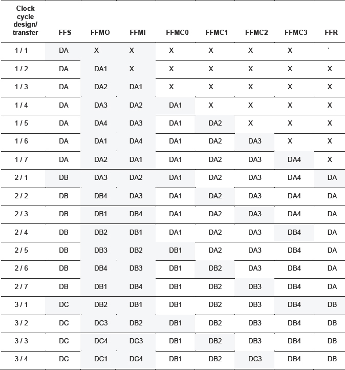
The shaded entries in the table show how the captured data bit is transported through the mux and dmux and is clocked into the receiving FFR. We have highlighted in capitals where each FF in the chain has new data.
As we can see from the first column of our tab, the ratio between the design clock and transfer clock is seven, which means that the design clock has to be seven times slower than the transfer clock to guarantee correct operation.

Now it is trivial to calculate the maximum design clock frequency for our synchronous multiplexing example:
So for this design, which multiplexes signals using a 4:1 mux ratio at 100MHz, we can run our design at over 14.28 MHz worst case, not the 25MHz that we might have guessed from the 4:1 ratio.
We have now seen the case where the transfer clock and the design clock are synchronous but let us consider the difference in an asynchronous multiplexing scheme where the design clock and the transfer clock are not phase aligned. The maximum transfer clock frequency is the same but we don’t know the skew between the active edges of the design and transfer clock. Therefore we have to add additional synchronization time on the send and receive sides to guarantee that we meet set-up and hold time between design and transfer clocks. This adds an additional transfer clock cycle on both send and receive sides. The calculation of the maximum design frequency for the asynchronous multiplexing is:

We can see that the asynchronous case runs with a lower design frequency but the advantage of asynchronous multiplexing is that we don’t need to synchronize the design and transfer clock and we have greater freedom from where to source the transfer clock.
To summarize the example, the important things we should keep in mind to constrain a design with multiplexing are:
- Calculate the correct maximum frequency of the transfer clock based on FPGA IO technologies, delays on board and tolerances.
- Calculate the correct ratio between design and transfer clock, respecting the difference between synchronous or asynchronous multiplexing.
- Give correct constraints in synthesis and FPGA place & route for the transfer clock and the design clock.
- Give correct clock-to-clock constraints in synthesis and FPGA place & route for the delay between transfer clock and design clock.
Having considered different kinds of multiplexing using normal single-ended signaling between the FPGAs, what can we do to have higher mux ratios but still maintain a high system speed? The answer lies in raising the maximum transfer clock speed, using the FPGA’s built-in serial IP and a more robust signaling technology.
8.7.5. Scheme based on LVDS and IOSERDES
We can further improve the transfer of data by sending the clock on a parallel path to the data. This method of sending clock and data together is called a source-synchronous interface. This makes it easier to meet timing because the clock has the same off-chip/on-chip skew as the data, especially if a well-designed board is used upon which there are matched delay traces with the same flight time.
Having the clock travel from the source, rather than be generated locally and kept in sync, would not work for driving partitioned logic in general but it is very useful for unidirectional serial data transfer.
Trace flight time works in our favor but it still places a physical limit on the maximum system speed and the way to overcome this is to use differential signaling between the FPGAs.
In this advanced case, we use the FPGA’s built-in support for LVDS, which can increase transfer rates up to 1GHz. This allows much higher mux ratios without having to reduce the overall prototype clock speed. Certify’s HSTDM scheme, briefly mentioned earlier, supports LVDS signaling but also uses another of the FPGA’s built-in resources, the IOSERDES blocks.
As introduced in chapter 3, modern FPGAs have dedicated serial-to-parallel converters called IOSERDES which have specific clocking and logic features for implementing high-speed serial transfers. Using IOSERDES avoids the timing and layout complexities of implementing the similar functionality within the FPGA fabric.
We can also double our transmitted data rate by using both edges of the transfer clock using the FPGA’s built-in support for double data rate (DDR) operation of the IOSERDES blocks. Figure 122 gives an overview of the implementation of a highspeed TDM scheme which combines all of these advanced built-in features of a Virtex-6 FPGA.
LVDS guarantees the highest transfer speed on-board but the slight disadvantage is that there are two pins required for each serialized data stream. So, while a single-ended multiplexing scheme with a ratio of 8:1 needs only one inter-FPGA trace to transfer eight data signals, a differential IO standard needs two, so we call this a mux ratio of 8:2. Therefore the differential solution reduces the interconnections only by factor four and not by factor eight. However, when the significantly higher speed of LVDS is taken into account then multiplexing ratios of 128:2 can be considered, which gives a far greater data transfer bandwidth than is possible with a single-ended scheme.
As shown in the diagram, this IOSERDES is being run at a transfer rate of 400MHz and needs two clocks for operation. The clocks are generated from a PLL within the source FPGA based on a 100MHz clock arriving from an external source. The OSERDES is configured as an 8:1 ratio but because it operates in DDR mode, we need only have a transfer clock of 400MHz rather than 800MHz. This means that the 400MHz clock transfers 8 bits during one 100MHz period. To provide multiplexing ratios higher than eight we can use an additional mux at the input of the OSERDES but this only needs to work at the slower internal clock rate.
Figure 122: Advanced multiplexing scheme using LVDS and IOSERDES
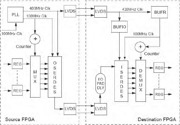
The data and the transfer clock are both passed to the destination FPGA via LVDS signaling but at the destination FPGA only the data goes through an IODELAY element to adjust its timing relative to the clock. The data and the transfer clock then drive the ISERDES block. Received clock is passed through BUFR block to divide it by four to create the local version of the 100MHz, which is also required for the ISERDES and the dmux control.
The diagram gives only an overview and implementations may be more complex and include so-called link training of all HSTDM multiplexing channels in order to guarantee optimal alignment between clock and data. It is important that user data is not transferred over the link while training occurs and it would be lost in any case, so only after the link training is complete is a ready signal generated. This should be included as another input to the reset condition tree discussed in section 8.5 above. If such a training is not implemented the user has to manually adjust the IDELAY components to achieve highest speed and to guarantee the right operation.
8.7.6. Which multiplexing scheme is best for our design?
Given the number of options, it may be difficult to decide which multiplexing scheme is the best to use in our prototyping project. To help us, Table 21 shows a comparison of the multiplexing schemes described in the above sections.
Table 21: High-level comparison between multiplexing schemes
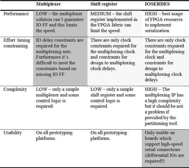
The comparisons are shaded with the least preferable under each criterion shaded darker. As we can see in the comparison, the shift register solution is a flexible, easy to handle solution and can be used on all prototyping platforms. However, let’s not lose sight of our goal of enabling the highest transfer speed so that the prototype speed is not compromised too much. Therefore the IOSERDES solution may be offer a greater reward, but the effort may be higher and the board/system needs to support LVDS signaling across matched-delay traces.
8.8. Timing constraints for multiplexing schemes
If multiplexing is used then we need to add timing constraints for the mux and interconnects so that the implementation tools will consider them along with those for the rest of the design.
The most obvious constraint is the clock constraint for the mux clock. Based on the multiplexing scheme used and the required performance of the prototyping system, it should be possible to analyze the maximum possible transfer clock speed and then work backwards to calculate the optimum constraint accordingly. Some partitioning tools can perform timing estimation if they can be given information about the board trace delays. The derived clock constraint for the transfer clock can then be used during synthesis and place & route.
We can calculate the maximum design speed based on the maximum transfer clock speed. Remember that the mux transfers exactly one set of its inputs to the destination FPGA within a design clock period but the ratio of mux clock to design clock depends not only on the multiplexing ratio but also on the multiplexing scheme used and any skew and jitter margin added between design clock and transfer clock. The clock-to-clock ratio, rather than just the mux ratio, should be provided by the designer of the multiplexing scheme in use.
Other required constraints are the maximum delay constraints between the design clock domain and the transfer clock domain. As we have seen before, the ratio between design clock and transfer clock depends on the delay between design and the multiplexing components. If we assume that there is a defined delay like 10ns we have to give a constraint to the place & route tools to ensure that all multiplexed connections are within this range. This kind of constraint is often missing but it is important to guarantee full functionality. See the worked example above for how to calculate the correct constraint.
If we perform multiplexing correctly, all timing will be met, a high performance will be achieved and the end user of the prototype should not even be aware that multiplexing has been used.
8.9. Partitioning and reconnection: summary
For many FPGA-based prototyping teams, the first law of prototyping, that “SoC’s are larger than FPGAs,” drives the whole project. As we have seen, if a design has not been intended at all for prototyping and has a large and complex internal structure, then partitioning it into our board’s FPGA resources can present quite a challenge, and if we cannot partition our design then the project will fail. However, even with such pathologically FPGA-hostile designs, a way for it to be partitioned onto a board can be found with the question only being a matter of time allowed versus how much performance is required.
By following an FPMM-based approach and the steps given in this chapter, we give ourselves every chance of not only fitting the design onto the board but also of running it at maximum speed, even if we need to use multiplexing between the FPGAs.
There is an old joke about a lost driver stopping to ask a local pedestrian how to find his way to London, to which the local replied, “Oh, you don’t want to start from here!”
We would all prefer a more predictable partitioning outcome so we can make an earlier delivery of our working prototypes to the end users. Therefore we don’t want to start from an SoC design that is complex, interconnected with multiple wide buses and many inter-dependent functions. But how do we get these better starting places? How can we make prototyping more productive?
What if prototypers could take part in more of the upstream decisions of the SoC project team and guide the design towards something less hostile to FPGA, thus breaking the third law of prototyping at its source? That is the aim of the discussion in chapter 9, Design-for-Prototyping, where we consider some small procedural and technical changes in the SoC flow which will bring benefits to the whole team, not just to us prototypers… honest!
The authors gratefully acknowledge significant contribution to this chapter from
Pradeep Gothi of Synopsys, Bangalore