CHAPTER 7 |
GETTING THE |
This chapter describes the main prototyping challenges, common practices and the process of taking an SoC design into the FPGA-based prototyping system. It covers SoC design-related issues, techniques to make the design prototyping friendly and how to use FPGA special-purpose resources. We cover SoC library cells, memories and clock gating in depth. We also revisit the implementation process and common tools outlined in chapter 3 in order to accomplish the best system performance.
7.1. Why “get the design ready to prototype?”
While the aim is always to prototype the SoC source RTL in its original form, early on in the prototyping effort it typically becomes evident that the SoC design will have to be modified for it to fit into the prototyping system. The design variations are typically due to design elements found in the SoC technology which are not available in, or suitable for FPGA technology. Design variations are also caused by limitations in the prototyping platform, tweaking for higher performance and debug instrumentation. The typical design variations, and examples of how to best handle them, are discussed in more detail later in this chapter.
To facilitate the SoC design modifications, we may make copies of affected source files, edit them and then simply replace the originals for the duration of the prototyping project. Obviously care and revision control methods should be employed to avoid error but in the end, we are probably going to be changing the RTL at some time.
7.1.1. RTL modifications for prototyping
Table 15: SoC design elements that might require RTL changes
| Top-level pads | Instantiations of SoC pads will not be understood by the FPGA tool flow. |
| Gate-level netlists | The design is not available in RTL form, but only as a mapped netlist of SoC library cells. These will not be understood by the FPGA tool flow. |
| SoC cell instantiations | Leaf cells from the SoC library are instantiated into the RTL, for whatever reason, and they will also not be understood by the FPGA tool flow. |
| SoC memories | Instantiations of SoC memory will not be understood by the FPGA tool flow. |
| SoC-specific IP | From simple DesignWare macros up to full CPU sub-systems, if the source RTL for the IP is not available then we will need to insert an equivalent. |
| BIST | Built-in self test (BIST) and other test-related circuitry is mostly inferred during the SoC flow but some is also instantiated directly into the RTL. This is not required for the prototype and may not be understood by the tools. |
| Gated clocks | As with BIST, clock gating can be inferred by SoC tools but is often written directly into the RTL. This generally overflows the clock resources available in the FPGAs. |
| Complex generated clocks | As with gated clocks, generated clocks might require simplification or otherwise handling in order to fit into the FPGA. |
The most common elements in SoC designs that need to be modified during prototyping include those listed in Table 15.
In addition, there are other reasons why we might need to alter the original RTL, including test-point insertion, tie-off of unused inputs, instantiation of FPGA-specific clocks etc. Each of these types of RTL change will be explained in the following pages and we will give some practical ways to implement them.
7.2. Adapting the design’s top level
We asked ourselves a rhetorical question in chapter 4 which was: “how much of the design should we prototype?” and it is time to answer that question in more detail. We will find a number of technology-specific elements that will not work in our FPGAs, usually at the top level of an SoC design hierarchy. These are the chip support elements and the top-level IO pad instantiations. A rough diagram of an SoC top-level is shown in Figure 66 where we see the SoC-specific chip support alongside the majority of the SoC logic in the core block, which is the top of the rest of the design hierarchy.
Figure 66: Simplified view of SoC top-level
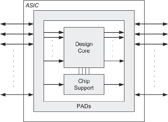
To introduce this design into FPGA, we will need to either replace the chip support and IO pads with FPGA equivalents, or simply remove the top level entirely and wrap the design core with a new FPGA-specific top level. We will address the chip support block in a moment, but first, how do we handle the IO?
7.2.1. Handling the IO pads
FPGA synthesis does not need to have IO pad instantiations in the RTL because it is able to infer an FPGA pad and even configure it in most cases, using only the defaults or simple attributes attached to the top-level signal. We could therefore simply leave the pads out and tie the dangling connections inactive or to the top-level boundary as required.
An alternative approach is to leave the IP pad ring in place and to replace each IO pad instance with a synthesizable model of its FPGA equivalent.
A typical IO pad from a silicon technology library may have 20 or more connections at its boundary, including the main input and output plus voltage and slew controls and scan test. Some of these connections will link to the package pins/balls while others connect into the core of the design or directly to adjacent pads.
For the purposes of prototyping, we need only model the logical connection from the design core to the “outside” world. Therefore, we need only a simpler form of the pad which makes that logical connection, omitting the scan etc. We can easily make a small RTL file which fits into the IO pad instantiation in the SoC RTL but contains the FPGA subset equivalent. This converts a black box pad instantiation into something that the FPGA synthesis can use.
Although there may be over a thousand pads in the SoC, there may be only ten or so different types of pad. Replacing each type with an FPGA equivalent will be relatively simple, especially if our SoC designs use the same pad library over multiple projects and we can build up a small library of equivalents.
7.2.2. Handling top-level chip support elements
The block in Figure 66, labeled “Chip Support,” contains those elements in the design that are generally target specific, often seen as secondary to the main function of the RTL, and yet are essential to its correct operation. This might include such functions as clock generation and distribution, reset control and synchronization, power-gating control and test and debug control. How much of this is relevant for our prototype or is even needed for an FPGA implementation?
Some teams recommend simply replacing the chip support block with another, simpler block which takes care of those elements needed for the FPGAs. This means that, in effect we have a new FPGA-compatible version of the top-level of the SoC. The top-level RTL file for the SoC can be used as the basis for the new FPGA top-level and an example of what the new top-level might look like is shown in the block diagram in Figure 67.
Here we see the clock generation and synchronization circuits at the top level supporting the existing design core. The creation of the equivalent FPGA chip support block is a relatively simple FPGA design task involving dividers, clock buffers and synchronizers, as shown in Figure 68.
Figure 67: New design top-level for prototype
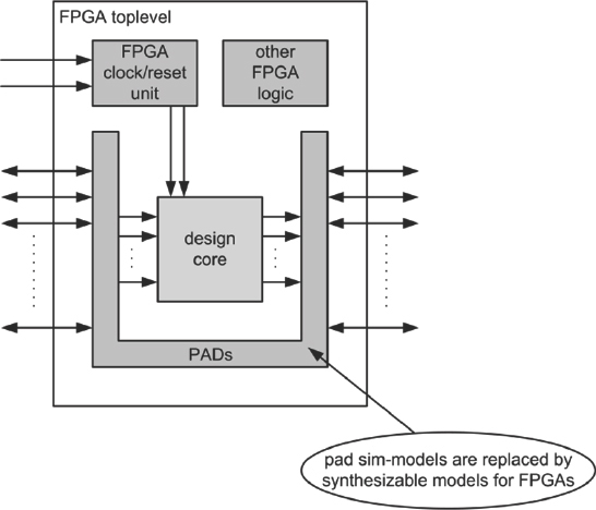
The use of the FPGA clock networks becomes more complex when the prototype uses multiple FPGAs so we shall revisit the top-level again in chapter 8, where we explore partitioned designs.
Let’s look now more closely at how we handle clock gating, one of the most important tasks in making a design FPGA-ready.
Figure 68: Simple illustration of top-level chip support block for FPGA implementation
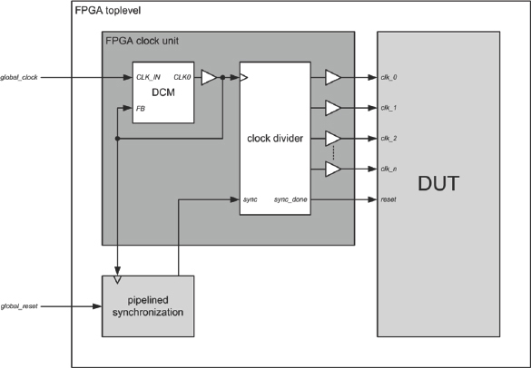
7.3. Clock gating
Clock gating is a methodology of turning off the clock for a particular block when it is not needed and is used by most SoC designs today as an effective technique to save dynamic power. In SoC designs clock gating may be done at two levels:
- Clock RTL gating is designed into the SoC architecture and coded as part of the RTL functionality. It stops the clocks for individual blocks when those blocks are inactive, effectively disabling all functionality of those blocks. Because large blocks of logic are not switching for many cycles it saves substantial dynamic power. The simplest and most common form of clock gating is when a logical “AND” function is used to selectively disable the clock to individual blocks by a control signal, as illustrated in Figure 69.
- During synthesis, the tools identify groups of FFs which share a common enable control signal and use them to selectively switch off the clocks to those groups of flops.
Figure 69: RTL clock gating in SoC to reduce dynamic power
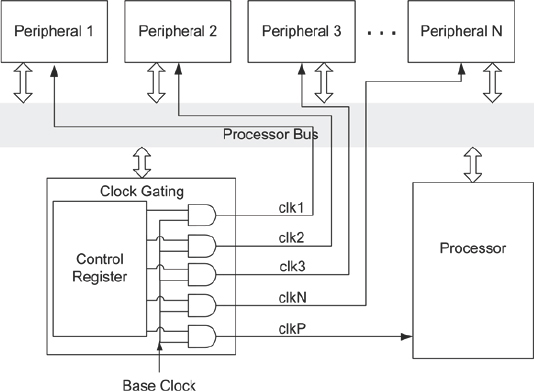
Both of these clock-gating methods will eventually introduce physical gates in the clock paths which control their downstream clocks. These gates could introduce clock skew and lead to setup and hold-time violations even when mapped into the SoC, however, this is compensated for by the clock-tree synthesis and layout tools at various stages of the SoC back-end flow. Clock-tree synthesis for SoC designs balances the clock buffering, segmentation and routing between the sources and destinations to ensure timing closure, even if those paths include clock gating.
This is not possible in FPGA technology, so some other method will be required to map the SoC design if it contains a large number of gated clocks or complex clock networks.
7.3.1. Problems of clock gating in FPGA
As we saw in chapter 3, all FPGA devices have dedicated low-skew clock tree networks called global clocks. These are limited in number, but they can clock all sequential resources in an FPGA at frequencies of many hundreds of megahertz. Owing to diligent chip design by the FPGA vendors, the clock networks also have skew of only a few tens of picoseconds between any two destinations in the FPGA. Therefore, it is always advisable to use these global clocks when we target a design into FPGAs.
However, FPGA clock resources are not suited to creating a large number of relatively small clock domains, such as we commonly find in SoCs. On the contrary, an FPGA is better suited to implementing a small number of large synchronous clock networks which can be considered global across the device.
Global clock networks are very useful, but may not be flexible enough to represent the clocking needs of a sophisticated SoC design, especially if the clock gating is performed in the RTL. This is because physical gates are introduced into the clock paths by the clock-gating procedure and the global clock lines cannot naturally accommodate these physical gates. As a consequence, the place & route tools will be forced to use other on-chip routing resources for the clock networks with inserted gates, usually resulting in large clock skews between different paths to destination registers.
A possible exception to this happens when architecture-level clock gating is employed in the SoC, for example when using coarse-grained on-off control for clocks in order to reduce dynamic power consumption. In those cases it may be possible to partition all the loads for the gated clock into the same FPGA and drive them from the same clock driver block. The clock driver blocks in the latest FPGAs, for example, the clock management tiles (CMT) in Virtex-6 devices with their mixed-mode clock managers (MMCMs) have different controls to allow control of the clock output. Some clock-domain on-off control could be modeled using this coarse-grained capability of the CMT.
In some SoC designs there may also be paths in the design with source and destination FFs driven by different related clocks e.g., a clock and a derived gated clock created by a physical gate in the clock path, as shown in Figure 70. It is quite possible that the data from the source FF will reach the destination FF quicker/later than the gated clock, and this race condition can lead to timing violations.
7.3.2. Converting gated clocks
The solution to the above race condition is to separate the base clock and gating from the gated clock. Then route the separated base clock to the clock and gating to the clock enables of all the sequential elements. When the clock is to be switched “on,” the sequential elements will be enabled and when the clock is to be switched “off,” the sequential elements will be disabled. Typically, many gated clocks are derived from the same base clock, so separating the gating from the clock allows a single global clock line to be used for many gated clocks. This way the functionality
is preserved and logic gates present in the clock path are moved into the datapath, which eliminates the clock skew as illustrated in Figure 70.
Figure 70: Gated clock conversion and how it eliminates clock skew
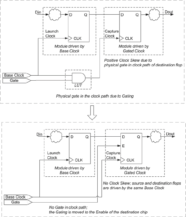
This process is called gated clock conversion. All the sequential elements in an FPGA have dedicated clock-enable inputs so in most of the cases, the gated clock conversion could use this and not require any extra FPGA resource. However, manually converting gated clocks to equivalent enables is a difficult and error-prone process, although it could be made a little easier if the clock gating in the SoC design were all performed at the same place in the design hierarchy, rather than scattered throughout various sub-functions.
As we saw in Figure 66 earlier, the chip support block at the top level could include all the clock generation and clock gating necessary to drive the whole SoC. Then, during prototyping, this chip support block can be replaced with its FPGA equivalent. At the same time, we can manually replace the clock gates, either instantiated or inferred, with an enable signal which can routed throughout the device. This would then perform the role of enabling only a single edge of the global clock at each time that the original gated clock would have risen.
In most cases, manual manipulation is not possible owing to complexity, for example, if clocks are gated locally at many different always or process blocks in the RTL. In that case, and probably as the default in most design flows, automated gated-clock conversion can be employed.
7.4. Automatic gated-clock conversion
Modern FPGA synthesis tools perform this gated-clock conversion process automatically without us having to change the RTL, however, we may need to guide the synthesis tools appropriately to perform the gated-clock conversion. It should be noted that some tools are more capable than others in this task.
Here are some of the guidelines to make the synthesis tools convert the gated clocks successfully.
- Identify the base clocks and define them to the synthesis tool by adding frequency or period constraints.
- Do not define the downstream gated clocks as clocks. Remove any period or frequency constraints on the gated clocks, which may have been specified during the SoC flow.
- Set any necessary controls in the synthesis tools to enable gated-clock conversion.
- Identify any black boxes in the design which are driven by gated clocks. To fix gated clocks that drive black boxes, the clock and clock-enable signal inputs to the black boxes must be identified. Synthesis tool specific directives should be used to identify them.
- If there are combinatorial loops in the clock-gating logic then the combinatorial loops should be broken. This can be done by inserting a feed-through black box, which is a black box with one input and one output and is placed in the combinatorial loop paths as shown in Figure 71. We can then create a separate netlist for the black box with the output simply connected to input. And the created netlist for the black box must then be added to the design during place and route.
Figure 71: Interrupting combinatorial loops to enable clock gating
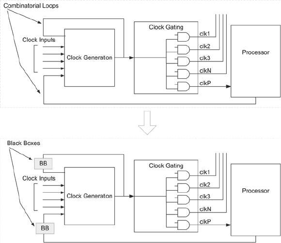
When all the above guidelines are followed then the synthesis tools can automatically convert all the convertible gated clocks.
The gated clock is convertible when all of the following conditions are met.
- For certain combinations of the gating signals, the gated-clock output must be capable of being disabled.
- For the remaining combinations of the gating signals, the gated-clock output should equal either the base clock or its inverted value.
- The gated clock is derived based on only one base clock.
Figure 72: Examples of convertible and non-convertible clock gates
Convertible |
When the value of Gate input is 0, the Gated CLK output is disabled. When the value of Gate is 1, the Gated CLK follows the Base CLK. This satisfies all the conditions. So AND logic is convertible. |
Non Convertible |
Gated CLK output cannot be disabled for either of the values of the Gate input. This violates the first condition and hence XOR is not convertible. |
Non-convertible |
Gated CLK is derived based on two base clocks. This violates the third condition and hence MUX is not automatically convertible. |
In order to illustrate these guidelines, Figure 72 gives some examples of simple convertible and non-convertible gates.
FPGA synthesis tools report all the converted and non-converted sequential components in its log files. The tools also list the reasons why the conversion did not happen for the non-converted sequential components. It is always advisable to look at these reports to make sure that the gated-clock conversion had happened for all the necessary sequential components.
7.4.1. Handling non-convertible gating logic
For an SoC design to work reliably on an FPGA-based prototype, all the gated clocks in the design should be converted. If the gated clock is derived based on multiple clocks, or the gating logic is complex, then synthesis tools cannot do the gated-clock conversion. However, these scenarios are sometimes common in SoC designs which can lead to many setup and hold-time violations. Here are some of the ways in which these scenarios can be handled. Use all these methods collectively as applicable.
- If there are no paths between the sequential elements driven by the base clocks and the unconverted gated clock, then the latter will not create any cross-domain timing violations. However, their routing in the FPGA may need to be carefully controlled to avoid the races described above.
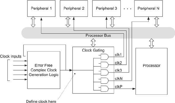
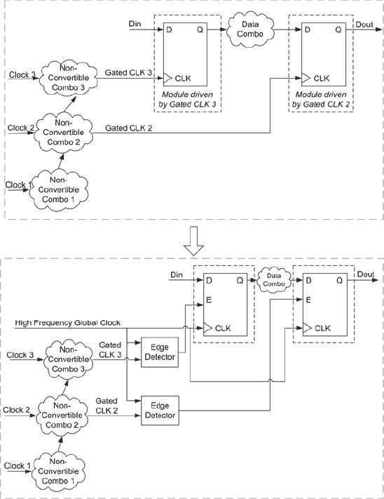
An intermediate node in the design can be identified and defined as a base clock such that the gating logic present, driven by that node, is convertible. Usually, SoC designs will have a clock-generation logic block with complicated logic to generate a glitch free, fail-safe and error-free clock. This clock will be created based on switching between many different clocks. And this generated clock will be used as the base clock for the rest of the blocks in the design with individual gating logic. Defining the clock on the output of the clock-generation logic block will make sure that all the gated clocks created, based on this clock, will be converted by the synthesis tool as shown in care must be taken in the layout of these edge detectors during place and route to avoid introducing differential delay between the paths clk_reg1 and clk_reg2. Use the outputs of these edge detectors as enables on all the sequential elements which were originally driven by the corresponding gated/generated clocks.
- Figure 73.
Figure 73: Handling complex clock gating
- If there are valid timing paths between one base clock and its complex gated clock, then try to manually balance the clock paths between these paths. It can be balanced by introducing feed-through LUTs, clock buffers, PLLs and digital clock managers in one of the clock paths.
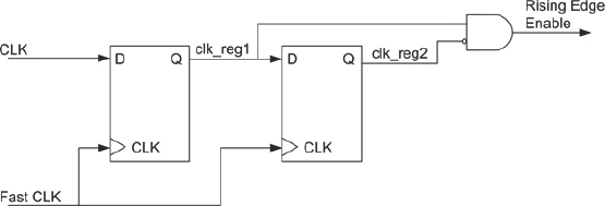
- If there are still some gated clocks which are not converted, and there are huge valid timing violations, then try to run all the sequential elements in the FPGA at very high frequency – around 10x the fastest clock in the design. Insert rising-edge detectors with respect to the faster clock for all the gated clocks in the design. This rising-edge detector can be designed by double registering (say clk_reg1 and clk_reg2) the gated-clock signals using the faster clock and then forming a logic to detect the change from LOW to HIGH (NOT(clk_reg2) AND clk_reg1) as shown in
- Figure 74. If the original clock drives FFs which operate on a negative edge also, then negative-edge detector circuits will also be required.
Figure 74: Rising edge detector
In this way, the whole of the FPGA is driven by a single faster clock source as shown in Figure 75. This clock will use the dedicated global routing resources in the FPGA and therefore the associated clock skew will be very minimal and the timing can be easily met.
Figure 75: Handling complex clock gating with global clock
7.4.2. Clock gating summary
Clock gating is common in SoC designs and gated clocks should be handled with care to successfully prototype the SoC designs on FPGA. Contemporary FPGA synthesis tools automatically take care of most of these gated clocks when properly constrained. By following the guidelines in this chapter, SoC designs with complex clock gating can also be handled and successfully prototyped in FPGAs.
7.5. Selecting a subset of the design for prototyping
Most SoC designs include SoC technology elements that are not available in FPGA technology such as PLL, analog circuitry, BIST, SoC primitives and third-party IP. The following paragraphs describe some options to deal with SoC design elements that do not map into FPGA.
7.5.1. SoC block removal and its effect
In the cases where SoC design elements are not available in FPGA technology, or where there is no desire to prototype certain blocks, these blocks need to be removed from the design. The removal may be as simple as removing a complete RTL design file from the project, leaving an unpaired module definition which might be inferred automatically as a black box. Alternatively, the RTL design file may need to be replaced with a dummy file which explicitly includes the necessary directive to set the module as a black box for synthesis.
In less tidy arrangements, the element to be removed may be buried in an RTL file alongside other logic that we wish to keep. In that case it may be necessary to alter the RTL, but a better approach, as we shall see in chapter 9, would be to predict at the time that the RTL was written that the element might need to be removed.
Figure 76: removing a block from the design using ifdef
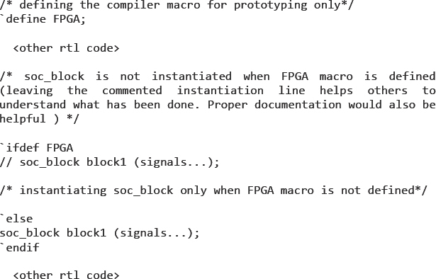
Taking this approach, a conditional branch may have been placed into the original RTL code, based on a single macro. The example in Figure 76 shows the condition removal of a module using define and ifdef.
The rest of the design that would normally connect with the removed logic may be handled in different ways by different synthesis tools. Some tools will simply flag the condition as an error error-out because there are dangling connections, but other tools will also remove downstream logic which is not driven as a result of the change; either up to a block boundary or other synthesis-invariant point, up to and including the entire cone of downstream logic. Upstream, that logic which previously drove the removed block will also be pruned as far as any upstream sources which also drive other, non-pruned, cones of logic.
To illustrate this effect, let us consider the small excerpt from a design shown in Figure 77.
Figure 77: Typical excerpt of logic before block removal
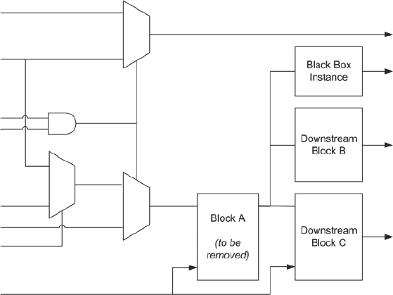
Let us suppose that Block A is not required in the prototype so we intend to simply remove it and allow the synthesis to prune out the unnecessary logic. The ripple-out effect of Block A’s removal upstream and downstream will depend upon the synthesis tool’s defaults and configuration. In Figure 78 we see that for a specific synthesis tool set-up, the upstream and downstream logic is mostly pruned as we might expect. Block A is removed along with all mutually exclusive upstream logic.
The AND gate is the point at which pruning stops because it is also driving other logic.
Downstream, two effects are instructive. Firstly, the downstream blocks receiving inputs from the removed block will be removed in turn unless they also receive data inputs from other parts of the design (clock or reset inputs are not sufficient). So in our example, Block B is completely removed, probably causing further pruning of ITS downstream logic. Block C will undergo pruning because some internal logic will not be driven when Block A is removed, while some other logic will remain because it is driven from other sources.
Figure 78: Effect of removing Block A from Figure 77 and resultant pruning
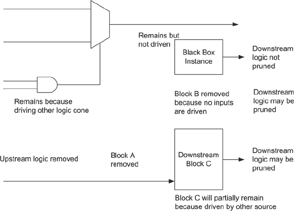
The second item of note is that the black box may not be removed by default and neit her will its downstream logic, with the consequence that back-end tools will need to handle the lack of inputs, which may or may not be possible. This can manifest itself in some very subtle ways, for example, an instantiated BlockRAM may survive until place and route and then prevent completion because of non-driven inputs. Even worse may be the setting of non-driven inputs to unexpected values and the BlockRAM remains in circuit.
Thus, we should take care with simple removal of blocks as a method for reducing the size of our prototype. Trimming of upstream logic which is unique to the removed block is not usually a problem; however, pruning of downstream logic may have widespread and unpredictable effects.
Synthesis tool settings for cross-boundary optimizations will have an effect to promote or prevent the ripple-out of logic removal. There may also be tool-specific directives and attributes within the design or project files or the tool itself which control logic pruning. Readers are encouraged to explore their own FPGA synthesis tools in order to understand their behavior in these circumstances. For the Synopsys® example, Synplify Pro® synthesis tools have a directive called syn_noprune which, as the name suggests, prevents pruning of non-terminated or non-driven signals.
However, even if such a directive is used in synthesis, it may be that the place & route tools will have their own default operation which overrides the setting when dangling signals are found in the input netlist. It is good practice to ensure that every system or toolset used for the project is explicitly given a predictable setup rather than rely on defaults. If the members of our SoC and/or prototyping project teams are running different tools installations and seeing different results in their respective labs, then tool defaults and settings are a good place to start looking for the reasons.
So, block removal is a quick and powerful way to remove unwanted logic but may have unforeseen results. A better approach may be to replace the block with a simple set of constant values called stubs, which leave no room for ambiguity of tool dependence. There is more detail on the use of stubs in the next section.
7.5.2. SoC element tie-off with stubs
To remove possible ambiguity between tool-flows as a result of element removal, as discussed above, a simple step is to add a dummy design file which explicitly ties-off unused ports to desired values. Amending the example in section 7.5.1 aboveabove, we arrive at the following code:
We see that the code is altered to call a different version of the SoC block that included the stubs which tie off outputs to specific values, controlling downstream pruning. Inputs to the stub block can be ignored with the upstream pruning taking place as normal, alternatively, dummy registers or other logic might be used to sink the input signals or bring to an external test point using global signal (see next section). Another advantage of using stubs is that it more fully defines the design for simulation purposes. Simulators have a much more particular requirement for complete RTL code and will often error-out on signals etc. by default.
Figure 79: Substituting stub block using ifdef
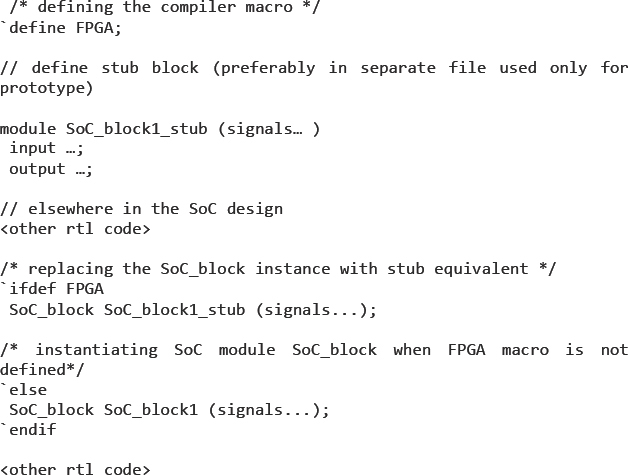
Therefore, stubs are a useful way to ensure repeatable pruning results, regardless of which tool we use or its setup.
7.5.3. Minimizing and localizing RTL changes
In previous examples, define and ifdef are used to control the synthesis branching between the FPGA and SoC code at compile time. In some cases, original RTL designers prefer to keep their code free of implementation-specific alterations. This fits within their team’s style guidance of separation and modularity. It is seen to be “cleaner” to keep as much target-specific code out of as much of the RTL as possible. In general, this also leads to a more adaptable design. There are a couple additional options that avoid unwanted ifdef’s but still improve the design’s adaptability.
As suggested in a few of the examples, one option is to create “libraries” for each target, for example, by isolating a sub-list of the source files that is target-specific and only including the relevant sub-list for a given target. The good points of this approach are that it allows us to quickly compare the two lists and discern where there are differences between the two databases. The strong disadvantage is that there are still two databases, and notwithstanding the naturally higher level of separation as compared to some of the other common approaches, maintaining multiple databases means more work and frequently leads to negligence of the secondary database.
This disadvantage is minimized if the target-specific code is kept as isolated as possible from the remaining code. For example, if several SoC library primitives are instantiated directly in a large module, two copies of the large module would have to be maintained. On the other hand, if the instantiation is of the library component (containing in one case the SoC primitive and in another case the synthesizable, behavioral equivalent), there is more chance that the code can change locally, without having to implement the change in multiple files.
Figure 80: Use of VHDL Global Signal to extract signal to a test point
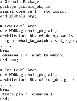
Some users find that the use of XMRs (cross-module references) in Verilog or Global signals, the VHDL equivalent, helps to decrease the scope of RTL changes. In Figure 80 we see an example of bringing an internal node out to a test pin using a VHDL Global signal. In this way we need change only three files and the only boundary change is at the top-level block in order to add the test pin itself.
Another good use of XMRs is to inject signals into a lower level. For example, one of the common needs in making a design FPGA-ready is to simplify clocking. To make this easier, SoC RTL writers are asked to keep clock generators, gates etc. in a common block at the top level. Their reason for not doing so is often that it would complicate the hierarchy boundaries to push the clocks down to the low-level modules where the clocks are used. XMRs can overcome that objection. XMRs may also be used retrospectively by the prototyping team to achieve much the same goal.
7.5.3.1. Note: netlist editing instead of RTL changes
Another approach is to use a netlist editing utility which may accompany some synthesis or partitioning tools. We explicitly specify the differences between the original database and any modifications required for the prototype directly in the synthesis netlist. The netlist editor would be run after each synthesis run, usually from a common script. This approach can be thought of as a series of overlays on the original RTL with the target-specific library compiled in parallel with the design and then stitched into the design using the netlist editor. This has all the advantages of the multiple filelist approach, maintains and utilizes the original golden SoC RTL without changes, and eliminates most issues associated with keeping RTL databases in sync.
Other approaches include using code generators and project generators. These are frequently written in Perl, C, etc., or using makefiles, or combinations thereof. In practice, most projects use combinations of approaches. For example, a project could use ifdef’s for the library selection, or include them in the library itself.
However it is done, the target-specific code should be architected so that it is tightly bound to local sections of the design. Keeping the effect close to the cause avoids confusion. The best approach is the one that minimizes the impact on the design and maximizes the ease and simplicity of switching between targets.
7.5.4. SoC element replacement with equivalent RTL
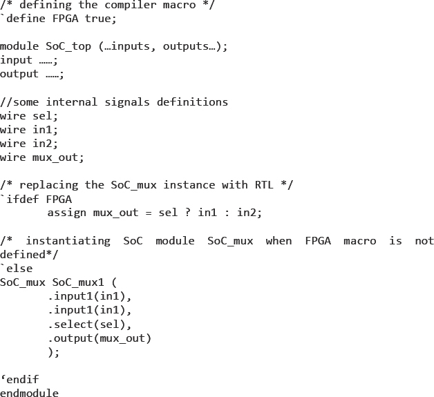
In the cases where a non-synthesizable SoC design element is needed in the FPGA-based prototyping effort, it may be replaced with synthesizable RTL code. In Figure 81 we see an example of an SoC primitive SoC_mux being replaced with RTL code:
It is obviously important to verify that the RTL is functionally equivalent to the SoC module it’s replacing. Therefore some simulation of the replacement alongside the original, perhaps with assertions checking for differences, would be very useful. We discuss such an approach with respect to memories in section 7.7.3 below.
Figure 81: Replacing instantiation with behavioral code
Recommendation: It’s important to note that if the remaining design is not properly terminated after removal of some blocks then the synthesis tool may optimize out (i.e., remove) any logic that is not driven by, or is not driving, other logic as a result. Therefore additional design modifications or synthesis directives may be necessary, such as creating stub designs.
In many cases the SoC element which requires replacement is an instantiated leaf cell from the technology library. A good source of equivalent functionality for such an instantiated SoC element can be found in the actual technology library used for the SoC.
The liberty (.lib) format for technology libraries includes an equation for the functionality for each leaf cell. We can see such a function for a basic cell in the small excerpt from a .lib file shown in
Figure 82 and we can see the function of the output pin Y in logical terms of the inputs. It is a simple matter to convert this “function” equation into equivalent RTL although there are EDA utilities which can perform the same task quickly and without error.
As an example, FPGA synthesis tools from Synopsys have the ability to read the .lib file directly and refer to the cell description in order to resolve instantiations of leaf cells in the RTL.
Figure 82: Excerpt from an AND-OR cell description in .lib file
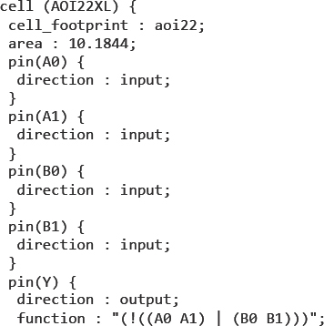
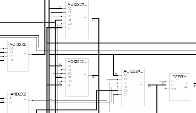
Figure 83 shows part of an RTL view of a gate-level netlist after being compiled into FPGA synthesis. Note that the blocks are leaf-cell elements from the technology library used for the SoC synthesis.
As noted previously, each of these cells would normally be interpreted by FPGA synthesis as a black box. Luckily, the source .lib file for the technology is available to the prototyping team and we can add this to our synthesis project as any other design file. The tools then automatically extract the functionality as mentioned, mapping it to FPGA resources during synthesis as normal.
Figure 83: Excerpt of graphical view of SoC gate-level netlist
If the .lib file is not available, or we are not using a synthesis tool that supports this flow, then a colleague supporting the SoC tool flow might be able to create a Verilog file from the .lib to add into the FPGA project. That Verilog file would only be a set of module definitions, which could be created using a utility such as Synopsys lib2syn, or even by a script which extracts the function from the .lib file and transcribes it into a Verilog module declaration.
7.5.5. SoC element replacement by inference
In some cases SoC elements can be substituted by equivalent FPGA design elements or “cores.” These FPGA cores are special-purpose FPGA entities used to optimize FPGA implementation for area and or performance. Common examples of FPGA primitives are memory blocks or shift register functions.
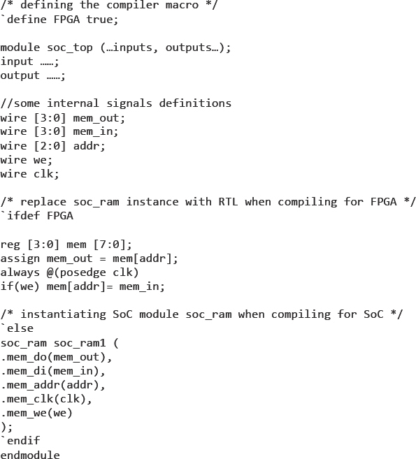
Usually, we do not need to simply replace an SoC element with an FPGA equivalent but instead we replace it with an RTL description and allow the synthesis tools to map it into FPGA elements by inference. The example in
Figure 84 shows an 8×4 synchronous RAM module soc_ram being replaced by RTL code. In this case, the FPGA memory block will be inferred by the synthesis tool during synthesis.
The RTL enabled by the FPGA macro will be interpreted by the FPGA synthesis as RAM and mapped into the relevant resource in the FPGA(s).
Figure 84: Instantiated RAM replaced by inferred equivalent
7.5.6. SoC element replacement by instantiation
In addition to memory blocks, FPGAs have some special-purpose blocks that may be needed for the prototyping effort. Examples of such blocks are high-speed serial interface blocks (also known as SERDES), DDR memory interfaces and FIFOs. Since these special-purpose blocks are highly programmable, they are not always inferred by the synthesis tools and instead they must be instantiated directly into the design.
The process of including such elements is as follows:
- Create an FPGA element using the FPGA vendor’s supplied tools (such as the Xilinx® CORE Generator™ tool, Memory Interface Generator etc.) Typically the user selects the core type, the target technology and defines the various parameters’ initial state values etc.
- The FPGA tool generates the desired core’s FPGA netlist and initialization file –where applicable – that are used in the place & route stage, and a template file used to instantiate the generated core into the main design.
- In addition, the tool generates a wrapper file containing functional simulation customization data that, combined with the primitive model used in the core, can be used for functional simulation.
- We then instantiate the template file in the design and connects the module to the design.
Figure 85: Instantiation template created by Xilinx® CORE Generator tool
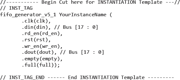
Figure 85 shows an instantiation of a FIFO template generated by the Xilinx® CORE Generator tool:
Figure 86: use of FIFO module in defined using the template in Figure 85
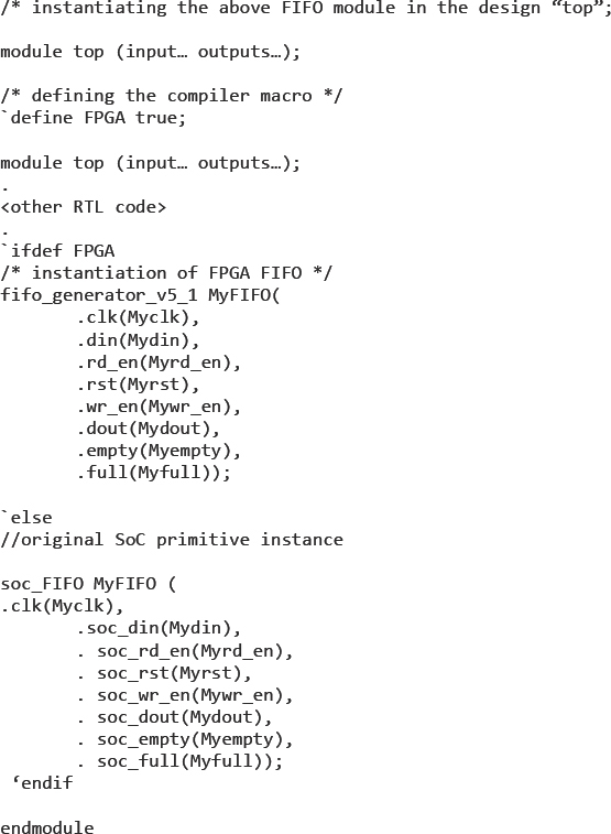
The FIFO template would be instantiated in place of SoC FIFO module as shown in Figure 86, once again using the FPGA macro to branch between implementations.
In the example, the synthesis tool will generate a netlist with an FPGA equivalent black box in place of the SoC black box. The contents are added in when the design reaches the back-end and the association is made by the model name in the template.
When instantiating a core for which an FPGA netlist exists, the synthesis tool usually applies timing constraints to the core. Furthermore, depending on the synthesis tool, it may also be possible to include the FPGA netlist during synthesis so that further optimization may occur. In this case, we refer to the module as a gray box.
7.5.7. Controlling inference using directives
There may be situations where within the same design the use of special-purpose FPGA resources is desired for some instances, but not desired for other instances. Such situations can happen due to the finite number of available resources or the locations of these resources and the way they are connected into the design. For example, in some Xilinx® FPGA families, dedicated 48-bit mult iplier blocks are available in fixed columns on the die. By default, the FPGA synthesis should map to dedicated resources but we also need to be able to override the default decisions in some situations. For example, when routing delays to a multiplier from the rest of the design placement would outweigh the performance gain in using it.
Figure 87: RTL excerpt showing control of DSP48 mapping using synthesis directive
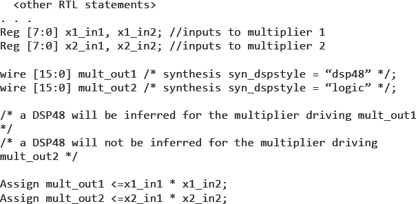
In that case it would be better instead to implement the multiply function in general-purpose distributed logic. So there is a need to selectively direct the synthesis tool to infer the dedicated multipliers for some multiply functions and to map to logic in other cases. A synthesis attribute should be available to control these kinds of decisions and override the default.
In the RTL in Figure 87 we see the use in Synopsys FPGA synthesis of an attribute called syn_dspstyle. This attribute can take one of two values: “logic” or “dsp48” and it is used to direct the synthesis to infer or not to infer the 48-bit fixed multiplier.
Note that this attribute also applies to other entities that can be mapped into the DSP48 block such as adders and registers.
In some cases, this process can be done automatically when synthesis infers the use of DSP and RAM blocks. The inference is timing-driven and often paths are retimed to get better DSP and RAM packing, but also a running count of DSP and RAM usage is maintained so that if the resource limit for the target FPGA is overflowed. Then some of the design that might otherwise infer DSP and RAM blocks will be automatically mapped into other logic resources instead.
7.6. Handling RAMs
Memory is the most common SoC element that requires some manipulation to be FPGA-ready. We will focus now on RAM in particular and consider other types of memory later.
We have seen in section 7.5.5 that RAM can be described behaviorally in RTL and then inferred by FPGA synthesis into the correct FPGA memory elements. Unfortunately, SoC synthesis tools do not handle memory in the same way, and instead they are instantiated as black boxes in the RTL. Various views, such as functional behavior and physical layout, are used to “fill” the black box later in the SoC verification and implementation flows.
These various views of the memory are often automatically created and parameterized by a generator such as the coreConsultant from Synopsys or Custom Touch Memory Compilers from Virage Logic. The SoC team will be familiar with these types of tools and use them to generate very sophisticated memories, optimized for the SoC design. In an ideal world, the FPGA synthesis would recognize the black box as the output from a particular memory generator and automatically replace it with an equivalent FPGA view. However, there are a large number of possible memory configurations, as can be seen in Table 16, and the synthesis would need to infer the functionality of each of them with only the reference of the black box name from external library as a guide.
Table 16: Examples of the wide range of RAMs in use in SoC designs
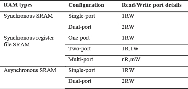
Maintaining a cross-reference of all possible SoC memories from all possible generators to their closest FPGA equivalent would not be productive and typically yields non-optimal results. Instead we focus on the specific RAMs in the SoC (which will be a small subset of the overall range of possible configurations) and create optimized replacements only for them.
Some help can be offered by the memory generator tools and memory IP developers themselves and some do indeed generate FPGA equivalent views for use by prototypers. In an ideal world our SoC team will have chosen their RAM for exactly that reason, but in most cases we need to consider how we can replace an SoC RAM with the FPGA equivalent.
7.7. Handling instantiated SoC RAM in FPGA
FPGA tools don’t understand any instantiated RAMs used in the SoC design. In addition, there are limits imposed by the memory architectures available in the FPGA device itself, so there is no guarantee that all types of SoC RAMs can be directly mapped into BlockRAMs or distributed RAMs that are supported in the FPGA device. Before exploring that further, here is a quick recap on FPGA RAMs (more details are in chapter 3).
7.7.1. Note: RAMs in Virtex®-6 FPGAs
In FPGAs, there are two different groups of RAMS; Block RAMs and distributed RAMs.
- BlockRAM: The Virtex®-6 block RAM stores up to 36K bits of data and can be configured as either two independent 18-Kbit RAMs, or one 36Kbit RAM. Each 36-Kbit BlockRAM can be configured in a number of ways e.g., 32K x 1, 16K x 2 etc. they can also be cascaded to create a 64Kx1 RAM. Each 18Kb BlockRAM can be configured as a 16K x 1, 8K x2, 4K x 4, 2K x 9, or 1K x 18 memory.
- Write and read are synchronous operations. The two ports are symmetrical and totally independent, sharing only the stored data. Each port can be configured in one of the available widths, independent of the other port. The memory content can be initialized or cleared by the configuration bitstream so that contents are already present when the device comes out of reset. During a write operation the memory can be set to have the data output either remain unchanged, reflect the new data being written or the previous data now being overwritten.
- The BlockRAMs may be configured as single-port, simple dual-port and true dual-port. Furthermore, embedded dual-port or single-port RAM modules, ROM modules, synchronous FIFOs, and data width converters are easily implemented from BlockRAMs using the Xilinx® CORE Generator™ module generator tool.
- Distributed RAM: The look-up tables in the FPGA can also be configured as RAM and because these are spread throughout the device, we call them distributed RAMs. With the use of surrounding logic, there is great flexibility in how distributed RAM can be used.
- In cases where the SoC RAM topology is not compatible with BlockRAM (e.g., quad-port or bit-addressable RAM) then distributed RAMs can be used. In any case, if the size of the RAM is small (e.g., 16×8, 36×2) then distributed RAMs are generally a better choice than BlockRAM.
- Interfaces to external RAM: FPGAs have a growing amount of internal RAM but it is inefficient to use up whole FPGAs just to map a few Megabytes of RAM from an ASIC. Furthermore, most SoC designs contain much larger RAMs than a few Megabytes, so for these reasons it will probably be necessary to map some of the SoC memory to external RAM components on the boards. FPGAs have the ability to interface through fast IO to external memories and even built-in support for interfacing to standard external RAMs, such as DDR2 and DDR3.
When mapping SoC RAMs it is necessary to adapt the RTL so that the FPGA tool flow can map it into the appropriate resource. We can do this without changing the existing RTL, but instead we add extra RTL files to act as an adaptor between the black-box RAM instantiations in the SoC RTL and the necessary FPGA or external equivalent. We call these adapters “wrappers” and we shall spend some time exploring their use next.
7.7.2. Using memory wrappers
A wrapper is a small piece of RTL that contains an item to be implemented in the FPGA, but which has a top-level boundary that maps to the component/module instantiation in the SoC RTL. Experienced prototypers will be very familiar with wrappers and may indeed have built up their own libraries of wrappers for use in various situations.
Figure 88: Basic concept of a wrapper for memory
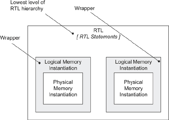
The diagram in Figure 88 shows the basic arrangement, in this case two wrappers used in the same level of hierarchy. Good practice in RTL would suggest that this would be at the lowest level of hierarchy of the SoC design but in the prototype, a wrapper adds levels below the logic already in place in the SoC. Strictly speaking this may break the style guide for the SoC project as a whole but may be preferable to editing the RTL in situ to add the new RAMs.
The simplest way to start creating a wrapper is to copy the component/module declaration from the SoC RTL and paste into a new RTL file. We shall later see what other items we might put in the wrapper body.
The first aim of a wrapper is to link the ports on the SoC RTL instantiation to the relevant ports on a module/component which the FPGA synthesis will understand as FPGA or external elements. This module/component may be a different black-box instantiation, for example a Xilinx® RAM macro or an external memory black box, or it may be another layer of hierarchy in which some new RTL infers an FPGA RAM.
7.7.2.1. Wrappers to instantiate equivalent FPGA RAMs
Figure 89 shows a schematic generated as an “RTL view” by Synopsys FPGA synthesis.
Figure 89: Typical wrapper for instantiate FPGA RAM as seen in Synplify® RTL View

Note that the port names of the top level, shown as page connectors in the schematic, are the same as the ports on the wrapper. This is not strictly necessary but careful choice of port names will make it easier for others to understand the intent and also some tools will be able to make additional associations by name. For example, during partitioning, the Certify® tool can associate the port names of an instantiated black box within the wrapper, with the pin names of the external memory as described on the board description (see chapter 8)
However, a wrapper can be more sophisticated and can be used to manipulate the SoC top-level ports into something that connects with rather different FPGA or external resources. For example, a wrapper might be written to merge input and output buses on an SoC RAM instantiation, into a common tri-state bus for connection to an external SRAM, as shown in Figure 90.
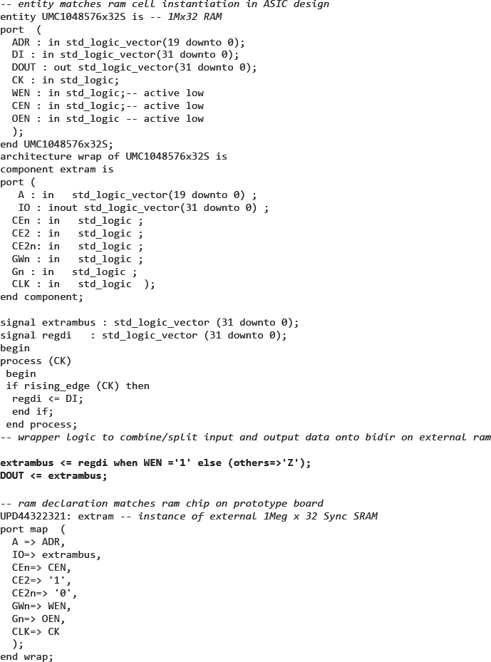
Here a 1Mx32 SoC RAM cell is being modeled with a small external memory device, using the RTL shown in Figure 91. Again, the top-level ports correspond with the RAM instantiation in the SoC RTL, the lower pin on “extram” correspond with the pin names on the RAM device as they appear in the board description.
Figure 90: Wrapper merging SoC RAM data ports onto bidir port on external RAM
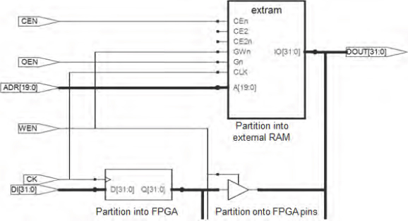
In this case both the RAM in the SoC and in the external device are named explicitly. We shall see later how we can make generic wrappers which allow parameterization and allow wider reuse for our wrappers.
Figure 91: VHDL code for wrapper shown in Figure 90 above
7.7.2.2. Tools for generating replacement memories
There are a number of tools which help to generate RAM and other memories for use in FPGA and we can use these for creating part of the contents for our wrapper. These tools are extensively used by FPGA designers for everyday production designs but can be equally useful for those using FPGAs only for prototyping. We will mention in particular two tools; CORE Generator tool from Xilinx and SYNCore from Synopsys.
CORE Generator tool creates memory models for implementation only in Xilinx® FPGA, the flow is typically to use the black box instantiation of the memory as created by CORE Generator tool and then the implementation is added-in automatically during place and route. The implementation of the memory (i.e., to fill the black box) is in a Xilinx-specific object format, called ngc, and might even be encrypted. The contents may be used by the synthesis tool if they can understand the ngc format. The FPGA elements can then be inspected for timing or physical information, which are both useful during FPGA synthesis.
Figure 92: Synopsys SYNCore memory compiler
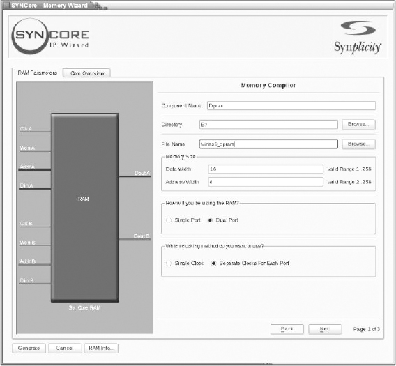
As an alternative to CORE Generator tool, Synplify Pro from Synopsys includes a sub-tool called the SYNCore IP Wizard. SYNCore generates portable parameterized RTL for IP elements including RAMs in different configurations such as single-port RAM, dual-port RAM and byte-enabled RAMs. Figure 92 shows a screenshot of SYNCore showing a dual-port RAM being created to target a Virtex-6 FPGA. In this case, the output is human readable Verilog RTL and so fully useable during all stages of FPGA synthesis and place and route.
Tools such as SYNCore and CORE Generator tool allow us to quickly generate the necessary internal FPGA RAMs and other memories for modeling the SoC instantiated memories, via the use of suitable wrappers.
7.7.2.3. Wrappers to infer equivalent RAMs
So far we have used wrappers to instantiate equivalent memories in place of the SoC instantiated memory. The memories generated by SYNCore, however, are actually in RTL from which FPGA synthesis can infer the required FPGA memory. This approach can be expanded to allow the creation of a small library of RTL descriptions which can be parameterized by the wrapper to create a large variety of different memories, for example, corresponding with the different types that we listed earlier in Table 16 (see page 195).
An RTL example for a paramaterized RAM is shown in Figure 93 on the next page.
Figure 93: Example of paramaterized generic RAM
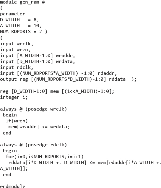
This example is a single-write and multiple-read RAM but the number of read ports can be changed by the NUM_RDPORTS parameter. Notice that the defaults in this example are used to set the number of read ports to two, but this would be overridden by a new parameter passed into the RTL from the hierarchy layer above. Synplify Pro would synthesize the above RTL into the RAM structure shown in Figure 94.
Figure 94: RAM structure inferred by RTL in Figure 93
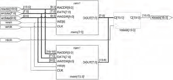
When mapped into BlockRAM in a Virtex-6 device, the rddata register bank would also be packed into the BlockRAM.
7.7.3. Advanced self-checking wrappers
We have so far considered two different kinds of wrappers. We have seen that some SoC designs do not use wrappers and instead instantiate the SoC memory directly into the surrounding RTL. In those cases, we need to use the SoC memory instantiation itself to define the top of the wrapper and place the FPGA or external equivalent in that.
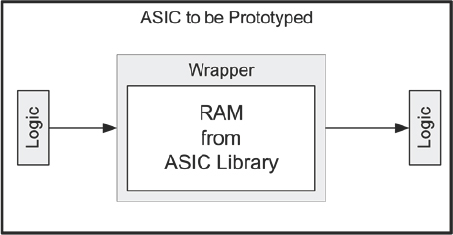
The second (and best) way to use memory in an SoC design is to put a wrapper around each instantiation, as shown in Figure 96. This requires that some foresight has been given to the needs of the prototypers and falls under the heading of Design-for-Prototyping, as we shall see in chapter 9.
Figure 96: Preferred wrapper in SoC design using Design-for-Prototyping
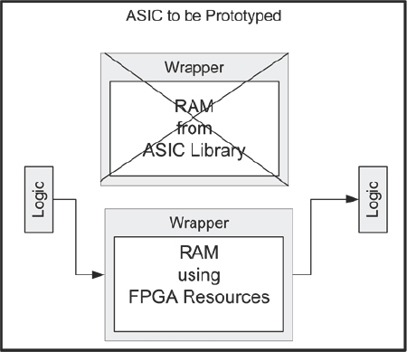
In normal prototype usage, we would replace the wrapper contents that instantiate the SoC memory with wrapper contents that instantiate or infer an FPGA equivalent, or an external chip, as shown in Figure 95.
Figure 95: Switching between wrappers using define fpga macro
Let’s now consider a special case where we have a wrapper which instantiates both the SoC memory and the FPGA memory at the same time.
An overview of this arrangement is shown in Figure 97 where we can see that both wrappers are present throughout the verification process and we only choose one during synthesis using the branching macro again. During verification runs, both the FPGA memory model and the SoC memory model are evaluated and assertions are used to compare the output of each, which should be functionally identical. Only the SoC memory’s result is passed to the rest of the logic. Wit hin reasonable limits this should not drastically increase the simulation runtime but we do get the benefit that the FPGA memory is thoroughly tested in all SoC verification runs before being used in the prototype.
Figure 97: Self-checking RAM model
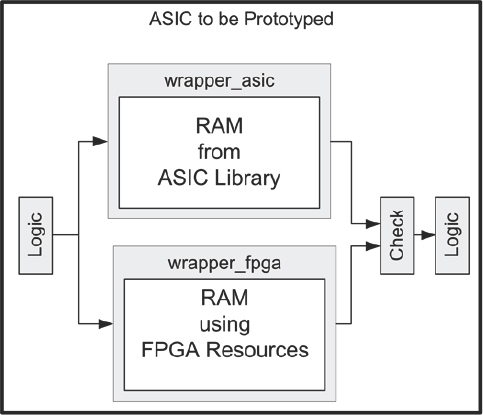
Using this approach, any discrepancies involved with assumptions on the RAM models between the SoC and FPGA versions can be found early in the design cycle, in fact even before synthesizing the design.
This methodology will require flow changes in the setup, and would definitely require that the SoC team embrace Design-for-Prototyping methods. Even if this requires some additional effort, we gain the advantage that memory modeling defects are found early in the design cycle.
We could also envisage a generic memory library in which for each memory used in SoC designs company-wide, we have a single file which encapsulates the RAM from ASIC Library, the equivalent RAM using FPGA resources and the equivalency check. If we maintain such a generic memory library then we would not need to make any RTL changes for most memories when it comes to prototyping.
7.8. Implementing more complex RAMs
What if the RAMs instantiated in the SoC design are too complex to be mapped to dedicated BlockRAMs? Do not despair. With some ingenuity we can usually find a way to use the FPGA memories and other resources to mimic the behavior that we require. We can do this in extra RTL that resides inside the wrappers and therefore does not need a change to the SoC RTL. We cannot possible explore all the possibilities here so we shall use two examples.
7.8.1. Example: implementing multiport RAMs
In the first case, let’s consider a register files used in an SoC design, configured with one write port and four read ports. To implement this in an FPGA, the synthesis tools would map this register file into normal FFs in the FPGA logic fabric. It would also use some LUT-based logic to perform decoding logic on the write port and for four multiplexers for the read ports. This may work very well for small register files but if such a structure were large enough, this could consume considerable amounts of logic.
Figure 98: Four BlockRAMs used to implement a quad-port register file
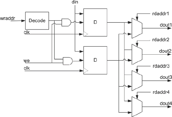
Alternatively, we could envisage an implementation where four BlockRAMs are used in parallel, as shown in the schematic in Figure 98.
Whether or not this is really a better use of resources depends upon which resource we have most to spare, logic or BlockRAMs. However, there is an approach we can take which uses only a single BlockRAM as shown in Figure 99.
Figure 99: Single BlockRAM used to implement a quad-port register file
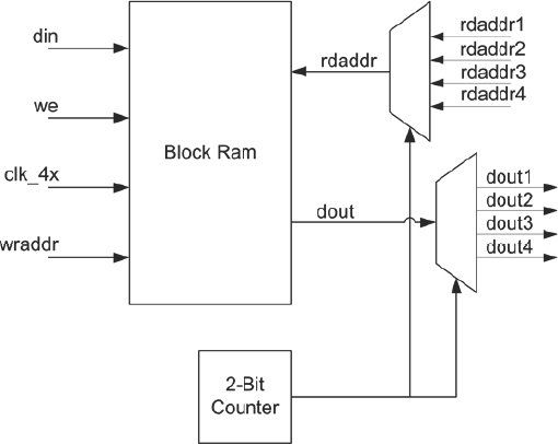
The BlockRAM and input and output multiplexers are clocked four times faster than the system clock. We then cycle a multiplexer at the higher clock rate to drive the four read ports using a four-to-one mux.
There would be a little extra logic overhead for muxing the read address and for generating the select signal for the output mux, but the overall resource usage would be lower than for either of the above implementations.
7.8.2. Example: bit-enabled RAMs
FPGA block memory resources are typically structured for byte-enabled writes so writing to a single bit would seem to be out of the question. However, there are a few techniques to build bit-enabled memories. One feature is to infer single-port and dual-port memories using the synthesis tool to map the bit-enables into the BlockRAM byte enables.
Figure 100, shows the paramaterized model for a single-port memory with a parameter to set the write size. We can see that parameters can be passed into the model for setting all the usual dimensions of the RAM, with their default values in case of omission.
Figure 100: Excerpt from paramaterized module to infer single-port RAM
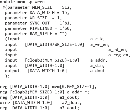
Figure 101: Wrapper for single-port RAM inference of SoC instantiation
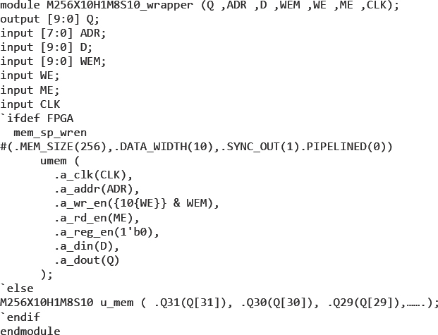
Figure 101 shows a wrapper for a bit-enabled single-port memory which either instantiates the model above with relevant parameters or instantiates the SoC RAM cell depending upon the value of the FPGA macro. The parameters for the model can often be extracted from the original SoC memory name, which usually follows some logical pattern. In this case, 256×10 is the memory depth and data width, H1M8S10 defines a single-port bit-enabled memory.
We can see from the port map that there is a parameter called RAM_STYLE for specifying the FPGA memory type to which the RAM will be mapped, taking the possible values: BlockRAM, distributed RAM or registers. If left unspecified, as in this example, the synthesis tool will pick the most efficient style at the time that the RAM is inferred. Typically, if the memory size is less than 256 it will infer distributed memories.
Figure 102 shows the RTL to handle the configurable write enables which could be of any width write. We can work through the RTL to see how the write enabling on less than the full BlockRAM width is performed.
When we come to bit-enabled dual-port and multi-port memories, these cannot be directly inferred into FPGA memory structures but once again, with some ingenuity when creating wrapper contents, we can find techniques for creating equivalent functionality.
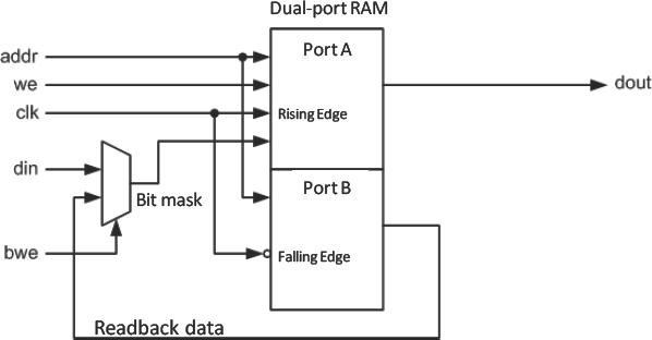
Our solution is a variation on the same technique used for standard multi-port memories that we described in section 7.6.1. Using a double-speed clock, a write cycle now consists of two fast clock cycles. On the first cycle, data is read from port
Figure 102: Excerpt of port logic within the model showing variable width write enable
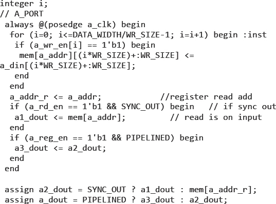
B using the same address to which we wish to write. This read-back data is presented to a gating structure which will mix it with the new data to be written. Then, on the second cycle, the write data to put into the RAM is chosen dependent on the bit-write enable mask. There is another variation on this idea shown in Figure 103 but here a 1W 2R port memory is used to construct a single-port bit-enabled memory, but instead of a high-speed clock, it uses both edges of the clock, falling for reads, rising for writes.
There are very many RAM topologies in use in modern SoC devices and the FPGA devices and tools infer many, but by no means all of them automatically. With our examples, we hope that we have illustrated that by good engineering we can always find a way to model the SoC RAM in the FPGA fabric, or by using external components on the board.
7.8.3. NOTE: using BlockRAM as ROMs
One feature of RAMs supported in the FPGA architecture is that they can be configured as ROMs because the RAM can be pre-loaded with desired values. This can be done at configuration time so that the FPGA comes out of reset with the RAM contents already defined. So for all intents, we have a ROM. Since the RAM is a synchronous element, any ROM created from it will have the same restrictions.
Figure 103: Bit-enabled dual-port memory using both edges of write clock
So any function that requires a look-up list of values needs to also have its outputs registered. If these restrictions are met, then the function can be mapped into a BlockRAM, saving LUT resources in the logic fabric of the FPGA. In many cases the synthesis tool can infer the use of ROM in this way from a suitable RTL descript ion.
7.9. Design implementation: synthesis
Once the design is made FPGA-ready, on the assumption that it fits into a single FPGA then we can move on to FPGA implementation, which as we saw in chapter 3, is comprised of synthesis and place and route (we shall deal in the next chapter about partitioning into multiple FPGAs, should that be necessary).
To recap, FPGA synthesis primarily compiles the RTL, checks for synthesis errors, accepts implementation constraints and generates FPGA netlists that are forwarded to the place & route tools along with further constraints.
To prepare our FPGA-ready design for synthesis, we must also enter the implementation constraints. These can be entered either in the design RTL itself or in the synthesis constraints files that can either be created directly by the user or by using a GUI provided by some tools.
The following are the most common implementation constraints:
- Device properties: these basic constraints direct the synthesis and subsequently the place & route tools to the FPGA family, specific device, speed grade and physical package.
- Pin locations and properties: this constraint maps each logical IO pin to a physical FPGA pin. The selection of pins is usually related to the prototyping platform architecture. If pin locations are not locked at this time then the pin assignment will change in subsequent synthesis runs and the design will not work in the FPGA. In addition to the physical pin location, we can specify IO properties such as signaling levels, slew rate, drive strengths etc.
- Timing constraints: this type of constraint is one of the most critical to the success of the prototyping effort. These constraints drive the synthesis and are passed on to the place & route tools to drive each towards the desired timing, balancing resource utilization and implementation effort. Timing constraints are usually entered in a synthesis constraints file, either manually or by using a GUI. Effective timing constraints will guide the implementation tools to put the effort where it is most needed. The most common timing constraints are: clock period, from/to delays, and multicycle paths.
- Other constraints: there are many other constraints and attributes that guide the synthesis and place & route tools, such as synthesis styles, state machine implementation styles etc. Good knowledge of the available attributes and how to apply them will help us to best leverage the tool and device capabilities to meet our prototyping goals.
7.9.1. Note: using existing constraints for the SoC design
In some cases the timing constraints for the original SoC design might be reusable to some degree in the FPGA-based prototyping flow. SoC synthesis tools, such as Design Compiler® (DC), will usually be configured in their project scripts to perform a bottom-up synthesis and so constraints are applied at each block level. However, there may often be top-level constraints which give at least the IO constraints for the device. There may even be a top-down flow employed in smaller designs, in which case the top-level timing constraints may be all that are available. In either case, the constraints will usually be written in a format called standard design constraint or SDC for short.
Advanced FPGA synthesis tools can make use of common timing constraints in the SDC format, thus allowing direct reuse of the same SoC constraints for the FPGAs in the prototype.
As an example, the following common design constrains are supported in Synopsys FPGA synthesis tools:
create_clock

create_generated_clock

set_clock_groups

set_input_delay

set_output_delay

set_false_path

set_multicycle_path

set_max_delay
These are the common set of timing constraints used in SoC designs and are fairly self explanatory from their names. Other unsupported constraints should either be manually translated (if a corresponding constraint is present in the FPGA synthesis tools) or ignored, depending upon importance. The tool documentation will give guidelines of the level of SDC support provided.
The SoC SDC will usually include much more than top-level timing constraints, for example “report” generation commands. Typically these are not directly supported or have a different syntax in the FPGA tools, so equivalent reports must be generated by using the timing analyzer capability within the FPGA synthesis and place & route tools manually.
To use the SDC timing constraints for FPGA synthesis in Synopsys FPGA synthesis tools, we need to take care of the naming rules employed. Names may change or be ambiguous between different tools, so some mismatch might occur between common naming conventions. All naming rules are configurable in Design Compiler and there are a wide variety of styles adopted by different SoC teams. For example, in the notation of hierarchy separators, naming of bus signals, multidimensional arrays, structures, records and generated signals and identifiers. If the naming conventions in the Design Compiler SDC do not match the default naming conventions followed in the FPGA synthesis tools, then we can explicitly add the appropriate command specifying the naming conventions in the beginning of the SDC file.
7.9.2. Tuning constraints
Tools will often have a constraint checker to allow a quick-pass analysis of coverage and legality of the constraints before running synthesis or place & route. The results are presented in a report which provides information on how the constraints will be interpreted by the tool, without having to wait for the tool to complete a full run. Based on the report, we can quickly edit the constraint file rather than wade through messages in a synthesis log file, which might run into many thousands of lines.
When synthesis is complete, the tools will provide reports giving details of utilization and estimated timing. These reports can give an early warning of design issues such as inter-FPGA critical paths, unexpected utilization levels and missing components. Although all timing is based only on estimates, synthesis reports should be carefully examined before proceeding to the place & route process as the design or constraints that may need to be modified. To ease this process, the reports can be examined automatically, either using the tool’s built-in report features or using scripts which search and manipulate the report files directly.
7.10. Prototyping power-saving features
In most cases, the power mitigation of an SoC is implemented by the use of scripts and control files outside of the RTL, in a language such as universal power format (UPF). The result of running UPF controls with SoC synthesis and back-end are that the RTL is modified and/or supplemented with extra circuitry. Generally, the prototyping team receives the RTL before this power mitigation work has taken place and it is still a pure description of the SoC function for prototyping purposes.
However, with the growth in sophistication of SoC power mitigation techniques, prototypers are sometimes asked if there is a way to test the RTL after the UPF and similar controls have inserted power-down modes, data retention and clock control.
Power modeling in FPGA is an interesting problem and not something that is easily implemented. Some functions obviously do not make sense in the FPGA, for example, the modeling of switching off the power to certain parts of the chip, but there is merit in prototyping some of the other properties.
It is possible to use the clock-gating features of synthesis tools to model some of the behavior, and careful use of PLLs can allow the frequency scaling features to be implemented, but adjustment of the supply voltage would not give any benefit, nor would the power monitoring of the core supply to the FPGA to determine power consumption as this would not be representative, and even worse give misleading results
However, it may be beneficial to use our prototype to model the power-control system itself and for this we would need to create some extra RTL, which would fool the power controls and the software into believing that the silicon was responding as expected. We can indeed dynamically adjust the frequency via internal or external PLLs. We could also mimic the expected responses of a voltage change or the effects of turning-off sections of the design. This might be useful for validating the software that controls such things but the complexity might far out way the benefit.
The model in its simplest mode would mimic the registers and interfaces seen in the real world and implement the time delays we would expect for the real system. However power gating sections of the design is more difficult as we would need to generate the impression that a section is powered down when the FPGA silicon cannot actually be powered down. For example, we would need to implement clock gating or other features to ensure that a section does not respond when it is meant to be switched off. It would also be impossible to represent the random values that might appear in SoC registers that are powered down because the FPGA registers would not actually have been powered down and will still hold valid values, perhaps masking an effect that would be very important to witness in the real sislicon. In these examples we see that perhaps, modeling SoC power-down features in FPGA might be more misleading than helpful.
To implement these features would either require RTL modification to the real SoC design (which is not ideal and should only be considered if really necessary) or the use of the ability of the Xilinx® FPGA device to be reconfigured (partial bitstreams with different INIT values may be loaded while the devices are operating, to determine if the changes in the values affect the design). It is not the aim of this book to explain partial reconfiguration, but further information can be found in the references.
Recommendation: prototyping is intended for creating a functional model of an SoC for software validation and system-level integration of software and hardware, pre-silicon. It performs this task best upon RTL which is delivered before it is manipulated for power saving or test purposes.
7.11. Design implementation: place & route
Place & route tools take the FPGA-level netlist, implementation constraints, and tool-specific directives generated by the synthesis tool, and perform mapping, and place & route to produce a bitfile to download into the FPGA on the board. If the design was properly constrained in the synthesis phase all implementation constraints will flow from the synthesis tool to the place and route tools. The user can provide a number of tool directives such as operational modes, effort levels, and reporting details to optimize its operation and reporting.
During the place & route process, the tools provide various intermediate status reports. Since for large designs the place & route process can take hours to complete, it is recommended that we review these intermediate reports as they become available and determine if the process is progressing as expected or if an intervention is needed. The following is a list of the critical reports typically generated through the place & route process:
- Mapping and utilization reports: these reports provide an account of the resources found in the design. These reports may indicate problems in the design if logic was unexpectedly removed etc. This can happen due to improper inclusion of cores as black boxes, or a cascading effect due to the removal of other blocks. To rectify such situations we should go back to the design and verify that the removed blocks are properly connected to the design after synthesis, that all cores are properly instantiated and all cores’ netlist files are available to the place & route tools.
- Preliminary timing report: usually before the full place & route process takes place, the tools estimate if the timing constraints are possible for the design. If for example, the number of combinatorial logic levels between two FFs is such that the time it will take to propagate through them is greater than the requested clock period, even with minimal routing delays, the tool may stop processing the design. In such case we need to understand the critical timing violations and determine if paths can be multi-cycle paths or make design changes to shorten them.
- Final timing report: this is the ultimate timing report for the design after the place & route process is complete. This report should be used to determine if the design meets the desired timing. If the timing results do not meet the requirements, the prototyping engineer needs to understand which paths are too long and rectify the issues either through tools’ performance parameters, tighter constraints, or design changes. It’s important to note that the timing reports are for each FPGA in isolation, and external timing analysis needs to be done, such as FPGA to FPGA and FPGA to other hardware. As mentioned in the “Design modifications due to prototyping system” section in this chapter, inserting FFs at all FPGA IOs will significantly optimize and simplify board-level timing calculations.
There are other manuals regarding the place and route of FPGA designs, including those in the references. In general, the default operation of place and route may suffice for some projects but as with all tool flows, exceptions will occur that require us to “roll up our sleeves” and become expert in some aspects of some tools. As discussed in chapter 4, FPGA-based prototyping is most successful when performed by FPGA experts.
7.12. Revision control during prototyping
As we have seen, although we try to minimize the impact of FPGA-based prototyping on the SoC source, we will probably need to make changes to the design files. As with all engineering tasks it is crucial to track and document these changes. In addition there may be changes to the embedded software running in our prototype or in simulation testbenches and of course, the prototyping tool set-up, scripts and so forth will need to be recorded in order to be repeatable. For all these reasons, the use of a revision-control system during prototyping will greatly assist us in recreating the prototype across platforms, sites and future derivative projects.
Undoubtedly, our labs already use revision control for hardware and software projects, and tools such as Perforce are widely used at Synopsys and Xilinx. When delivering RTL for use by the prototyping team, this is no less important to track than any other branching of the code. In parallel, the embedded software branches to run on the prototype may be very similar to that which will eventually run on the SoC (we certainly hope so) but there will be small changes, for example, a time constant in a header file to account for a slower clock. These small software changes must also be controlled and only the appropriate changes used for a particular prototype build.
This becomes exponentially more difficult to control when multiple engineers are working on the prototype and time is short. If we make changes to our branch of the SoC source code to enable prototyping or debug, then these will probably not be wanted back in the mainline SoC code repository. However, a change in an RTL file to fix a bug discovered during prototyping must obviously be fed back into the mainline code. Only good revision control will enable us to keep track and discriminate between these two cases.
We must resist the temptation to make quick and temporary changes during prototyping even though FPGAs offer great freedom to make exactly these kinds of quick changes. If we work with the mindset that anything we do can impact the final silicon, even though we are not working on the mainline of the code (either RTL or software), then we can avoid much unnecessary, inefficient and perhaps ultimately costly confusion.
7.13. Summary
In this chapter we have covered the bulk of the tasks we undertake n order to overcome the third law of prototyping. We have used a number of techniques to remove or at least neutralize elements of the SoC design which would not have worked as they are in FPGA. We hope that we have not discouraged readers from starting because even the most pathologically FPGA-hostile design can eventually be mapping onto an FPGA board.
Successful SoC prototyping demands a good understanding of FPGA technology and implementation tools, but most of all, we need to recognize which parts of the design will best respond to one or other of the above techniques.
The authors gratefully acknowledge significant contributions to this chapter from:
Steve Ravet of ARM, Austin
Joel Sandgathe of Microvision, Seattle
Pete Calabrese of Synopsys, Boston
Ramanan Sanjeevi Krishnan of Synopsys, Bangalore
Nithin Kumar Guggilla of Synopsys, Bangalore