CHAPTER 3 |
FPGA TECHNOLOGY |
This chapter’s focus is on the available technology, both hardware and software, for FPGA-based prototyping. It describes the main features of FPGAs as core technology and associated synthesis software technology as they pertain to FPGA-based prototyping. Following chapters describe how to use these technologies in greater detail. Firstly, describing current FPGA technology in general but focusing on the Xilinx® Virtex®-6 family. We will highlight the utility of each feature for FPGA-based prototyping, which depends not only on its functionality but also on its support in the relevant EDA tool.
3.1. FPGA device technology today
FPGAs devices are at the heart of the FPGA-based prototyping physical implementation. It is where the SoC design is going to be mapped and realized, so we really should take a close look at them and at the tools we use to work with them.
FPGAs have evolved over the years from modest (by today’s standard) programmable logic devices to very large logic arrays with versatile architectural features, running at impressive clock rates. A glimpse at Figure 20 shows in particular, the inexorable progress of FPGA capacity as architectures have improved and silicon technology has evolved in accordance with Moore’s Law. Indeed, those fabrication lines associated with producing FPGA devices for the main FPGA vendors, all of whom are fabless, have benefited from the experience of producing very large FPGA die and have been able to tune their processes accordingly. It should therefore be no surprise that FPGA progress has been in lockstep with the progress of silicon technology as a whole and we should expect it to at least continue to do so. In fact, at the time of writing, some exciting new developments are taking place with the use of 3D IC technology to allow some FPGAs to leap beyond Moore’s Law.
Figure 20: The evolution of FPGA technology
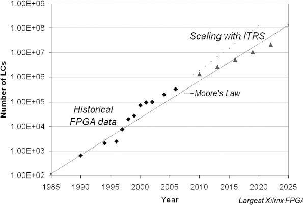
Investing in an FPGA-based prototyping approach should not be seen as involving any risk because of a scarcity of FPGA technology itself.
Let’s take a close look at a leading edge technology today; the Virtex®-6 family from Xilinx.
3.1.1. The Virtex®-6 family: an example of latest FPGAs
As our example in this chapter, we shall focus on Xilinx® FPGAs, since as of the writing of this chapter they are the most popular choice for FPGA-based prototyping across a wide section of the industry. The Xilinx® Virtex-6 family is currently the latest FPGA family from Xilinx, evolving from the Xilinx® Virtex®-5 architecture, but with enhanced features, greater capacity, improved performance and better power consumption.
As seen in Table 2, fabrication in a smaller CMOS process geometry enables more than doubling of logic capacity between the largest Virtex-5 and Virtex-6 devices but in addition, the ratio of FF (flip-flop) to logic resources has more than doubled, enabling better support for pipelined designs.
Table 2: Comparing largest Xilinx® Virtex®-5 and Virtex®-6 devices
| Feature | Virtex -5 | Virtex -6 |
| Logic Cells | 360,000 | 760,000 |
| FFs | 207,000 | 948,000 |
| BlockRAM | 18 MB | 38 MB |
Complete details of the devices and architectures is available by using some of the resources in the bibliography and appendices of this book, but let us spend some time now understanding each part of the FPGA technology, starting with the basic logic blocks and how helpful each may be towards our task of FPGA-based prototyping.
3.1.2. FPGA logic blocks
Sequential and combinatorial logic is implemented in logic blocks called slices. Slices contain look-up tables (LUTs), storage elements, and additional cascading logic.
Far more detail about FPGA technology is available in the references, but since the LUT is the fundamental building block in large FPGAs, it is worth a short examination here.
A typical 4-input LUT is at its heart a 16×1 RAM. Any particular bit of the RAM will be routed to the LUT’s output depending upon the 4-bit address. Now consider filling the 16 bits of RAM with various 1s and 0s so that when the address changes, so will the LUT output. We have created a logic function of four inputs and one output. All that remains is to so order the 16 bits of RAM to mimic a useful logic function. In fact, we can consider the 16 bits of RAM as a Karnaugh map and in the very early days, that was actually an option for programming them.
Thus logic functions, such as parity, XOR, AND, OR, and so forth, may be efficiently packed into the smallest number of LUTs to perform the desired function. Arithmet ic functions may also be placed in LUTs, and there is also hardwired carry look-ahead logic in the device so that performance may be improved over the use of LUTs alone.
Nowadays, we have up to 6-input LUTs (hence 64 bits of RAM) and it is all “programmed” via synthesis, which creates the LUT contents for us from a high-level description as required. Then the LUT RAM is loaded upon device configuration to create a complex 6-input function from just 64 bits of RAM. LUTs are embedded into other structures which include FFs, carry chains, arithmetic, memories and other sophisticated structures.
In a Xilinx® Virtex-6 device, LUTs are used to implement function generators of six independent inputs. Each six-input LUT has two outputs. These function generators can implement any arbitrarily defined boolean function of up to six inputs for the first output, and up to five inputs for the second output of the same LUT.
Two slices are combined into a configurable logic block (CLB). CLBs are arranged in the FPGA in an array, and are connected to each other and to other types of block via interconnect resources.
In Virtex-6 devices there are two types of slices:
- SLICEM - a slice in which its LUTs can be used to implement either combinatorial functions, a small RAM block or a shift register.
- SLICEL - a slice in which its LUTs can be used to implement combinatorial logic only.
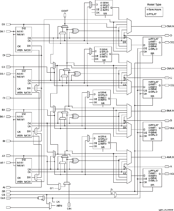
Figure 21 shows the SLICEM block diagram in which we can see that each slice contains four 6-input LUTs (on the left), eight storage elements (four FFs and four FF/Latches), and cascading logic. The various paths in the CLB can be programmed to connect or by-pass various combinations of the LUTs and FFs. Closer inspection also shows additional logic gates for particular carry and cascading functions which link resources within and outside the CLBs.
SLICEL is similar with the exception that the LUTs have only six input and two output signals. These resources can be configured for use as memory, most commonly RAM, and this is described briefly in section 3.1.3 below.
If the tools can make optimal use of the CLB in order to implement the design then the prototype will probably use less FPGA resources and run faster. This means that the tools must understand all the ways that the slice can be configured, and also what restrictions there may be on the use of the slice. For example, if the four FF/LAT storage elements are configured as latches, then the other four FFs cannot be used, hence designs which do not use latches are preferred. Also, control signals to the registers are shared so packing of design registers into slices becomes a complex task for the place & route tools if there are many different unrelated control signals in the design.
Figure 21: The Xilinx® Virtex®-6 SLICEM block diagram
As prototypers, we typically do not concern ourselves with the final usage of the various features of the slice because the implementation tools should automatically use an appropriate configuration in order to meet timing constraints. Having expertise to that level of detail may sometimes be necessary, however, so we recommend the references at the end of this book for further information.
Prototyping utility: very high, the essential building block. Synthesis will make good use of all the above features either automatically or under the direction of optional attributes and directives in the RTL and/or constraint files.
3.1.3. FPGA memory: LUT memory and block memory
SoC designs include multiple memories of various types, e.g., RAM, ROM, content-addressable. In the vast majority of cases, these will instantiated memories either from a cell library or from a memory generator utility. It is important that the FPGA can represent these memories as efficiently as possible. A selection of memory types are available in most high-end FPGAs, from small register files and shift registers, up to large scale RAMs. As we saw in section 3.1.2, the LUT in a Xilinx® Virtex-6 SLICEM logic block may be employed as a small local memory, for example, as a 32-bit bit-wide RAM. This allows significant freedom to implement the function of small memories found in many places in SoC designs.
Figure 22: Xilinx® Virtex®- 6 BlockRAM
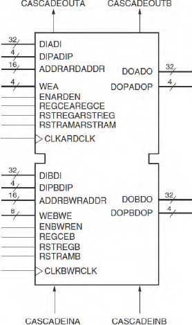
For the largest SoC memories, external memory resources are required. The FPGA’s own block memory resources will be very useful for smaller memories, and from a prototyping perspective, they are the second most critical resource in an FPGA. In the case of the Virtex-6 family, this memory resource is called BlockRAM and there are between 156 and 1064 BlockRAMs distributed throughout a Virtex-6 FPGA device.
A diagram of the Xilinx® Virtex-6 BlockRAM is shown in Figure 22
BlockRAMs have the following main features:
- Configurability: each block is a dedicated, dual-ported synchronous 36 Kbits RAM block that can be configured as 32K × 1, 16K × 2, 8K × 4, 4K × 9 (or 8), 2K × 18 (or 16), 1K × 36 (or 32), or 512 × 72 (or 64). Each port can be configured independently of the other.
- Synchronous operation: BlockRAMs can implement any single or dual ported synchronous memory. When configured as dual-ported RAM, each port can operate at a different clock rate.
- FIFO logic: dedicated – yet configurable – FIFO logic can be used in combination with BlockRAMs to implement address points and handshaking flags. FIFO logic’s depth and width can be configurable but both write and read sides must be the same width.
- ECC: when configured to 64-bit wide, each BlockRAM can store and utilize eight additional Hamming-code bits and perform single-bit error correction and double-bit error detection (ECC) during the read process. The ECC logic can also be used when writing to, or reading from external 64/72-bit wide memories.
BlockRAMs in the FPGA can be combined to model either deeper or wider memory SoC memories. This is commonly performed by the synthesis tools, which automatically partition larger memories into the multiple BlockRAMs. Some manipulation of the design from the SoC instantiation into the final FPGA BlockRAMs will be required and this is covered in detail in chapter 7.
Prototyping utility: BlockRAMs are major building blocks, inferred automatically by synthesis tools. At the time of writing, however, FIFO logic is not automatically supported by synthesis tools but can be included via core instantiation. For more details on memory implementation, refer to chapter 7.
3.1.4. FPGA DSP resources
SoC designs often contain arithmetic functions, such as multipliers, accumulators and other DSP logic. High-end FPGAs, such as the Xilinx® Virtex-6 devices address these needs by providing a finite number of dedicated DSP blocks; in the Virtex-6 family these are called DSP48E1 blocks. These are dedicated, configurable and low-power DSP slices combining high speed with small size, while retaining system design flexibility. Figure 23 shows a block diagram of the DSP48E1 in detail.
Figure 23: Xilinx® Virtex®-6 DSP48E1 Slice
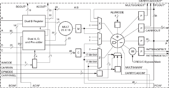
As shown in the block diagram, each DSP48E1 slice consists of a dedicated 25 × 18 bit two’s-complement multiplier and a 48-bit accumulator, both capable of operating at 600 MHz throughput. The multiplier can be dynamically bypassed, and two 48bit inputs can feed a single-instruction-mult iple-data (SIMD) arithmetic unit (dual 24-bit add/subtract/accumulate or quad 12-bit add/subtract/accumulate), or a logic unit that can generate any one of 10 different logic functions of the two operands.
The DSP48E1 includes an additional pre-adder, typically used in symmetrical filters. This feature improves performance in densely packed designs and helps reduce the number of logic slices that would be required before or after the DSP block to complete a specific topology.
The DSP48E1 slice provides extensive pipelining and extension capabilities such as wide dynamic bus shifters, memory address generators, wide bus multiplexers, and memory-mapped IO register files. The accumulator can also be used as a synchronous up/down counter. The multiplier can perform logic functions (AND, OR) and barrel shifting.
Prototyping utility: very high, a major building block. Most features are inferred automatically by synthesis tools, with the exception of pattern detect which can be included via core instantiation.
3.1.5. FPGA clocking resources
Clock resources and clock networks are a major differentiator between the FPGA and SoC technologies. Whereas SoC designers have almost complete freedom to specify as many clock networks as they can imagine of many varieties, there is a real and finite limit on how many of these can be implemented in an FPGA. The mapping of SoC clocks into FPGA clock resources can be the cause of significant project delays if not catered for properly by the SoC team, for example by providing a simplified version of the SoC clocking.
Prototyping is best performed on the RTL of the design before any clock tree synthesis, before tree segmentation for test and before clock manipulation for power reduction. Nevertheless, even the raw RTL from an SoC design may include some very sophisticated clock networks and the FPGA device will need to handle these. Indeed, in some designs, it is the finite number of clock resources in an FPGA that is the limiting factor, rather the device capacity or performance. It is therefore necessary to find a way to match FPGA clock resources to those of the SoC. This may be achieved by simplifying the original clock network (see Design-for-Prototyping recommendations in chapter 9) or by maximizing use of available FPGA clocks (see chapter 7).
Clocking resources can be divided into clock generation and clock distribution.
3.1.5.1. FPGA clock generation
Clocks are generated in configurable unit called CMT (clock management tile) which, in the Xilinx® Virtex-6 family, includes two mixed-mode clock managers (MMCMs). The MMCM is a multi-output frequency synthesizer based around a phase-locked loop (PLL) architecture with enhanced functions and capabilities. Each MMCM within the CMT can be treated separately; however, there exists a dedicated routing between MMCMs to allow more complex frequency synthesis. A diagram of the CMT is shown in Figure 24, giving a high-level view of the connection between the various clock input sources and the MMCM-to-MMCM connections.
The voltage controlled oscillator (VCO) in the PLL is capable of running in the 400MHz to 1600MHz range and minimum input frequency is as low as 10MHz, and has programmable frequency dividers and phase selection registers to provide output taps at 45° intervals.
Other programmable features include PLL bandwidth selection, fractional counters in either the feedback path (enabling the PLL to act as a clock multiplier) or in one output path, and fixed or dynamic phase shift in small increments.
Figure 24: Xilinx® Virtex®-6 Clock Management Tile (CMT)
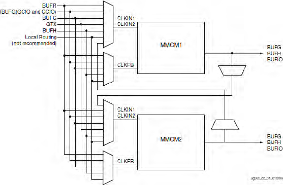
All this adds up to a very capable clock generation block and there are up to nine of these in each FPGA. We should therefore not be short of options when it comes to mapping SoC clock networks into the prototype.
Prototyping utility: very high, major building block. Many clock features are not inferred automatically and must be instantiated into an FPGA version of the RTL.
3.1.5.2. FPGA clock distribution
FPGA vendors, for decades, have put a great deal of effort into producing devices with as many clocks as possible yet without being wasteful of area resources. As a result, FPGAs are very good for implementing regular synchronous circuits with a finite number of clock networks. For efficiency, there is a hierarchy of different clock resources on most devices from global low-skew clocks down to local low-fanout clocks. Once again it is the task of synthesis and place & route to ensure good usage of these resources but also, manual intervention may be sometimes required to ease the task, as will be discussed in chapter 7.
In the case of the Xilinx® Virtex-6 family, each FPGA provides five different types of clock lines to address the different clocking requirements of high fanout, short propagation delay, and accomplish low skew across the device.
Xilinx® Virtex -6 clock distribution resources include:
- Global clock lines: each Virtex-6 FPGA has 32 global, high fanout clock lines that can reach every FF clock, clock enable, set/reset, as well as many logic inputs. There are 12 global clock lines within any region. Global clock lines can be driven by global clock buffers, which can also perform glitch-less clock multiplexing and the clock-enable function. Global clocks are often driven from the CMT, which can completely eliminate the basic clock distribution delay.
- Regional clocks: can drive all clock destinations in their region as well as the region above and below. A region is defined as any area that is 40 IOs and 40 CLBs high and half the chip wide. Virtex-6 FPGAs have between six and 18 regions. There are six regional clock tracks in every region. Each regional clock buffer can be driven from either of four clock-capable input pins and its frequency can optionally be divided by any integer from one to eight.
- IO clocks: especially fast clocks that serve only IO logic and serializer/deserializer (SERDES) circuits. Virtex-6 devices have a high-performance direct connection from the MMCM to the IO directly for low-jitter, high-performance interfaces.
Prototyping utility: very high, major building block, automatically inferred by synthesis tools. If regional clocks are required, then location constraints are often necessary in order to associate clock load with specific regions.
3.1.6. FPGA input and output
As we shall see later as we discuss multi-FPGA-based prototyping hardware, the ability to pass synchronous signals between FPGA devices, even to the point of multiplexing different signals onto the same wire, depends on the presence of fast and flexible IO pins and clocking resources at the FPGA boundaries. As with clocking, the finite number of IO pins can often be a more limiting factor than device capacity or internal performance.
In Xilinx® Virtex-6 devices there are 240 to 1200 IO pins depending on device and package size. Each IO pin is configurable and can comply with numerous IO standards, using up to 2.5V. With the exception of supply pins and a few dedicated configuration pins, all other package pins have the same IO capabilities, constrained only by certain banking/grouping rules.
All IO pins are organized in banks, with 40 pins per bank. Each bank has one common VCCO output supply-voltage pin, which also powers certain input buffers. Some single-ended input buffers require an externally applied reference voltage (VREF). There are two VREF pins per bank (except configuration bank 0). A single bank can have only one VREF voltage value.
Characteristics: single-ended outputs use a conventional CMOS push/pull output structure driving high towards VCCO or low towards ground, and can be put into high-Z state. In addition, the slew rate and the output strength are also programmable. The input is always active but is usually ignored while the output is active. Each pin can optionally have a weak pull-up or a weak pull-down resistor. Further details of the IO pins’ single-ended operation are:
- IO logic: each IO pin has an associated logic block in which a number of options can be selected:
- Configuration: all inputs and outputs can be configured as either combinatorial or registered. Double data rate (DDR) is supported by all inputs and outputs.
- Delay: any input or output can be individually delayed by up to 32 increments of ~78ps each. This is implemented as IODELAY. The number of delay steps can be set by configuration and can also be incremented or decremented dynamically while in use. IODELAY works with a frequency close to 200MHz. Each 32-tap total IODELAY is controlled by that frequency, thus unaffected by temperature, supply voltage, and processing variations.
- Drive current: the FPGAs might be required to interface to a wide variety of peripherals, some mounted on daughter cards that have yet to be created. Virtex-6 FPGA IO pins can be configured to support different drive strengths from 2mA up to 24mA .
Any pair of IO pins can be configured as differential input pair or output pair. Differential input pin pairs can optionally be terminated with a 100Ω internal resistor. All Xilinx® Virtex-6 devices support differential standards beyond LVDS: HT, RSDS, BLVDS, differential SSTL, and differential HSTL.
- ISERDES and OSERDES: SERDES blocks reside inside the IO structure. Each input has access to its own deserializer (serial-to-parallel converter) with programmable parallel width of 2, 3, 4, 5, 6, 7, 8, or 10 bits and each output has access to its own serializer (parallel-to-serial converter) with programmable parallel width of up to 8-bits wide for single data rate (SDR), or up to 10-bits wide for double data rate (DDR). We shall see in chapter 8 how the SERDES blocks can be used to great effect in enabling high-speed time-division multiplexing of signals between FPGAs.
There are other more complex IO blocks, such as gigabit transceivers and PCIe blocks and there are references in the bibliography where the reader can find out more about using these blocks for specific purposes in an FPGA-based prototype.
There is also discussion in chapter 10 about the use of built-in IP in the FPGA to mimic the IP in the SoC under test.
Prototyping utility: IOs are major building blocks for design top-level IO and for inter-FPGA connection. Default single ended and DDR IOs are automatically inferred. Different IO types are selected by attributes assignments in the synthesis constraint manager and then are passed to the place and route tools. IODELAYs, and IO SERDES can be included only via core instantiation.
3.1.7. Gigabit transceivers
Increasingly common in ASIC and SoC designs are fast serial communication channels, used to connect ICs over a backplane, or over longer distances. These are always instantiated as black boxes in the RTL design with references to physical IO elements in the final silicon layout. We shall see in later chapters how this might be handled in an FPGA-based prototype. To model these ultra-fast serial transceivers in an FPGA requires specialized and dedicated on-chip circuitry, including differential IO capable of coping with the signal integrity issues at these high data rates.
In the Xilinx® Virtex-6 family this high-speed serial IO is enabled by the presence of gigabit transceiver blocks, or GTX blocks for short. A detailed schematic of a GTX block is shown in Figure 25, which shows that as well as the physical transmit and receive buffers, the GTX blocks also have the ability to implement the physical media attachment (PMA) and physical coding sub-layer (PCS). Each GTX transceiver also has a large number of user-configurable features and parameters.
Each transceiver is a combined transmitter and receiver capable of operating at a data rate between 155Mb/s and 6.5Gb/s. Both the transmitter and receiver are independent circuits that use separate PLLs to multiply the reference frequency input by certain programmable numbers between two and 25, to become the bit-serial data clock.
Considering first the transmitter, this is fundamentally a parallel-to-serial converter with a conversion ratio of 8, 10, 16, 20, 32, or 40. The transmitter output drives the PC board with a single-channel differential current-mode logic (CML) output signal.
In its turn, the receiver is fundamentally a serial-to-parallel converter, converting the incoming bit-serial differential signal into a parallel stream of words, each 8, 10, 16, 20, 32, or 40-bits wide. The receiver takes the incoming differential data stream, feeds it through a programmable equalizer – to compensate for PC board and other interconnect characteristics – and uses the FREF input to initiate clock recognition.
Figure 25: Xilinx® Virtex®-6 GTX block schematic
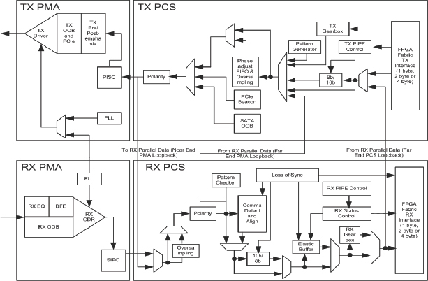
The different members of the Xilinx® Virtex-6 family have between 8 and 36 (GTX) circuits each with the exception of the largest device, the LX760, which does not have GTX capability. Therefore, if we need to prototype high-speed serial IP in our designs then some mix of FPGAs may be required and we shall explore this in chapter 5.
Prototyping utility: while a very powerful capability, due to their complexities and configurable options, GTX and their associated logic are not automatically inferred by synthesis tools. These blocks however, can be included via core instantiation.
3.1.8. Built-in IP (Ethernet, PCI Express®, CPU etc.)
Typically, many networking and communications SoC designs include Ethernet or PCI Express channels, so how would these be modeled in an FPGA-based prototype? FPGAs become ever more capable in their ability to implement standard interfaces at the MAC (Media Access Controller) and PHY (Physical interface transceiver). If the chosen FPGA has these capabilities built-in, then these can be used to substitute for those physical IP blocks which will eventually be embedded in the SoC but which probably appear as black boxes in the RTL. There is more information on this substitution in chapter 10.
In the case of Virtex-6 FPGAs, PCIe and Ethernet MAC and PHY are integrated into the FPGA fabric.
For Ethernet, there are up to four tri-Mode (10/100/1000 Mb/s) Ethernet MAC (TEMAC) blocks designed to the IEEE Std 802.3-2005. These can be connected to the FPGA logic, the GTX transceivers, and the IO resources and support speeds up to 2.5Gbit/sec.
For PCIe, all Xilinx® Virtex-6 LXT and SXT devices include an integrated interface block for PCI Express technology that can be configured as an endpoint or root port, designed to the PCIe base specification revision 2.0. This block is highly configurable to system design requirements and can operate 1, 2, 4, or 8 lanes at the 2.5Gbit/s data rate and the 5.0Gbit/s data rate.
Some FPGAs include CPU hard cores, often an ARM IP core of some kind. These are optimized for FPGA and will run at much higher speed than the RTL of the SoC equivalent when synthesized into FPGA, often by a factor of 10:1. Their usefulness for prototyping can be very high but only if the FPGA’s core matches the actual cores built into the SoC. In addition, most SoC designs today are running multiple CPU cores, often with different capabilities or configurations. With a single, hard CPU core in each FPGA, the partitioning criteria will be driven by the need to split the design with one CPU in each FPGA. This may not be ideal for running the bus and other common design elements so the advantage gained in CPU speed may not translate to significant gain in overall prototype speed.
If there is much compromise in replacing the SoC core with a limited subset in the FPGA, then we might be better off using an external test chip or compromising on CPU speed rather than functionality. There is more discussion on IP in prototyping in chapter 10. In any case, if the CPU core is available in the largest FPGA in the family so that we do no compromise total resources, then it does not harm us to have the CPU present and we might be able to use it in a future design. In some cases, where Design-for-Prototyping procedures have been adopted by a team, the SoC CPU might even be chosen because it has a very close equivalent available in a FPGA. Our manifesto for Design-for-Prototyping procedures, of which this is admittedly an extreme example, is included in chapter 9.
Prototyping utility: while very powerful capability, hard IP blocks are not automatically inferred by synthesis tools. These blocks however, can be included via core instantiation as replacement for SoC blocks.
3.1.9. System monitor
Prototype designs can exercise a large proportion of an FPGA at high speed, so power dissipation, heating, voltage rails etc. may come under stress, especially if the design is not performing as expected, or under the influence of a bug. As we shall see in the chapters about choosing or building FPGA platforms, a built-in monitor of the FPGAs in the working prototype can be crucial in avoiding damage due to incorrect operation.
Each Xilinx® Virtex-6 FPGA contains a system monitor circuit providing thermal and power supply status information. Sensor outputs are digitized by a 10-bit 200k sample-per-second analog-to-digital converter (ADC). This ADC can also be used to digitize up to 17 external analog input channels. The system monitor ADC utilizes an on-chip reference circuit. In addition, on-chip temperature and power supplies are monitored with a measurement accuracy of ±4°C and ±1% respectively.
By default, the system monitor continuously digitizes the output of all on-chip sensors. The most recent measurement results together with maximum and minimum readings are stored in dedicated registers for access at any time through the DRP or JTAG interfaces. Alarms limits can automatically indicate over temperature events and unacceptable power supply variation. A specified limit (for example: 125°C) can be used to initiate an automatic power down.
The system monitor does not require explicit instantiation in a design. Once the appropriate power supply connections are made, measurement data can be accessed at any time, even before configuration or during power down, through the JTAG test access port (TAP).
We will see in chapter 5 how the system monitor can be used on a prototype board.
Prototyping utility: this block is primarily a “house-keeping” monitor, usually external to the actual design, and typically used via the JTAG chain to read the device and system’s health. It does however offer a unique opportunity to include ADC in the design and if desired can be included via core instantiation. For more details on core instantiation, refer to Chapter 10.
3.1.10. Summary of all FPGA resource types
Before we move on to the tools and flows in FPGA-based prototyping, let us summarize the different FPGA resources that we have highlighted so far and their usefulness for prototyping.
Table 3 summarizes the different blocks found in most large-scale FPGAs today. All FPGA resources are useful or indeed they would not be there in the first place, however, they are aimed at a wide range of users who employ their FPGAs in real world production applications. Their usefulness in prototyping SoCs will depend upon the ease with which the SoC elements can be mapped into them and the compromise which may be required to do so. Let us now look closely, then, at the tools which enable us to use these FPGA resources to our best ability during an FPGA-based prototyping project.
Table 3: Summary of usefulness of various FPGA resources
| Resource | Utility for prototyping | Inferred? |
| Logic Blocks | Very high, the essential building block | Always |
| RAM Blocks | High major building block | Usually |
| DSP Blocks | High, major building block. | Usually (some IP instantiation) |
| Clock Generation | Very high, an essential but limited resource | Often (may need RTL change) |
| Clock Distribution | Very high, global nets are precious resource | Usually |
| General IO | Very high, an essential and precious resource | Always (type set by attribute) |
| Fast Serial IO | High, useful for prototyping standard IP blocks | Seldom (requires IP instantiation) |
| Hard IP | Very powerful blocks but utility is design dependent. | Never (requires IP instantiation) |
| System Monitor | High, will protect investment in FPGA hardware | Never (requires design in) |
3.2. FPGA–based Prototyping process overview
Figure 26 shows the basic flow that we follow in the FPGA-based prototyping process: Let’s quickly look at each of these steps in turn.
- Synthesis: may e performed before or after partitioning. The process of converting RTL into an FPGA netlist. The synthesis process generates an FPGA netlist for the device of choice, and the implementation constraints to be used by the FPGA back-end tools. In addition, some synthesis tools provide early estimation of the expected performance, which allows the user to make changes to the design or constraints before spending any time in the potentially lengthy back-end process.
- Design adaptation for FPGA: in this step, the SoC RTL design is modified to better fit the FPGA technology and the specific prototyping platform. Typical modifications to the SoC RTL include the removal of blocks not to be prototyped, replacing some SoC-specific structures with FPGA structures like clock generation and other IP, and resizing blocks like memories to better fit in FPGA.
- Partitioning: the process in which the FPGA-ready version of the SoC RTL design is divided into blocks that map into individual FPGAs. This step is needed for designs that do not fit into a single FPGA. Partitioning can be done manually or using partitioning tools. A number of approaches to partitioning were explored in chapter 3.
- Constraint generation: this is a convenient point in the flow to enter the various implementation constraints such as timing and pin placements. Although constraints may be generated and applied to the back-end tools after synthesis, doing so prior to the synthesis step allows synthesis to produce an FPGA netlist that is more optimized to meet the area/speed constraints after place & route.
- Place & route: the process of converting the FPGA netlist and the user constraints into an FPGA bit stream which will be loaded into the FPGA to provide it with the design functionality. This is often simply referred to as place & route, but in fact involves a number of steps such as mapping, place & route and timing analysis.
Figure 26 Basic FPGA-based Prototyping flow
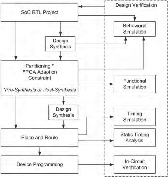
We will take a closer look in particular at all of the implementation steps but we do not plan to cover the verification stages in this book except to recommend that as much as possible of the existing SoC verification framework is maintained for use during the prototyping project.
At all points in the flow it is important to have ways to verify our work to that point. Re-using the original RTL testbenches and setup may require some adaptation to match the partitioned design. For example, after partitioning, a top-level netlist is required to link the partitioned FPGA netlists into a whole SoC design; often this top-level can be generated by the partitioning tools themselves.
Even if not for the whole design but for only sub-functions, maintaining a verification framework will pay us back later when we need to check functional issues seen in the design on the bench.
3.3. Implementation tools needed during prototyping
We have now explored the capability of the FPGA devices in some detail but these are of little interest if they cannot be readily employed in our prototype project. In the prototyping utility boxes above we have already mentioned that some resources are automatically employed whereas others will need some particular consideration. The ability of EDA tools for FPGA to make good use of the device resources is equally important as the resources themselves. We will now give an overview of the main EDA tools in the FPGA flow today, namely synthesis tools, partitioning tools, place & route tools and debug tools. We aim to keep the explanations as generic as possible and in each case give only small examples of tools from our own companies. More specific detail on tools available from Synopsys® and Xilinx® is available via the references. There is also more detail on the use of the tools in other chapters, particularly in chapters 7, 8 and 11.
3.3.1. Synthesis tools
As with almost every EDA tool flow, at the heart we find synthesis. For FPGA-based prototyping, we find synthesis converting the SoC RTL into a number of FPGA netlists to be used by the back-end tools, which then finally place and route the FPGA. However, at the same time the synthesis process is expected to infer regular structures from the RTL, optimize them and efficiently map them into the FPGA, meeting both space and performance goals.
As a brief illustration of this process, Figure 27 shows a screenshot of a Synopsys FPGA synthesis tool, and three views of the same small ALU design. In the bottom left is a text editor showing the RTL and the behavior extracted from that during the first stage of synthesis is shown above it. We can see a mux selecting the result of three different operations upon the inputs dependent upon an opcode and its output passing to a register. On the right of the screenshot we see a part of the final logic created by the synthesis, in particular note the use of LUTs for the multiplexing, FFs for the register and a DSP48 block used by default to implement the multiplier.
Figure 27: Synplify Pro® FPGA synthesis screenshot
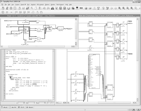
In the above example, we might decide that we do not want to waste such a powerful resource as a DSP48 block to implement a simple multiplier, so we could add an extra command, called an attribute, into the RTL or a parallel constraint file in order to override the default mapping. This is exactly the kind of control that a synthesis user has upon the way that the RTL is interpreted and implemented.
Let us a look a little more closely at the way that synthesis maps RTL to FPGA resources.
3.3.2. Mapping SoC design elements into FPGA
This section describes the tool’s features that support mapping of the SoC design into an FPGA, making use of our example FPGA devices from the Xilinx® Virtex-6 family. Many of the FPGA’s resources are supported transparently to the user because the synthesis tool automatically infers FPGA structures to implement user’s RTL with minimal or no intervention by the user.
3.3.2.1. Logic mapping
As logic is the primary resource for logic prototyping, mapping RTL into CLBs is an elementary function. For example, for the Xilinx® Virtex-6 architecture, synthesis should be able to do the following:
- Infer LUT6 where up to six input functions are needed. LUTs will be cascaded or split when more or less inputs are needed. For example, dual LUT5s will be inferred automatically when two functions sharing up to five common inputs can occupy the same CLB.
- Memory usage in SLICEM type slices will be inferred to implement distributed RAM and fast shift registers.
- Clock enables will be inferred, with the ability to re-wire low-fanout clock enable to LUTS to maximize slice utilization.
- Set/reset, synchronous or asynchronous will be inferred including prevention/arbitration of simultaneous set/reset assertion, avoiding unpredictable behavior in silicon. For example, Synplify Pro detects such a possibility, issues a warning and then generates a logically equivalent single asynchronous reset logic.
3.3.2.2. Memory block mapping
SoC designs include many and varied memory elements and we need to map these efficiently to avoid wasting our FPGA resources. Synthesis should be able to perform the following:
- Automatically infer single and dual ported memory structures into block RAMs.
- Pack adjacent input and output registers of pipeline stages into the BlockRAMs automatically.
- Make use of BlockRAM operational modes including read-first, write-first and no-change: preserving the initial value of either of the RAM’s input or output ports – as required to match the SoC’s behavior.
- Automatically split larger memories beyond the capacity of a BlockRAM into multiple blocks and add the necessary logic to split and merge address and data as required. The topology of the split (i.e., optimized for speed or area) should also be controllable.
3.3.2.3. DSP block mapping
Many SoC designs include blocks which make extensive use of arithmetic and algorithmic function. If the tools can map these into the DSP blocks in the FPGA by default then a significant proportion of the FPGA resources can be liberated for other purposes.
- Adders/subtractors: FPGA logic elements have simple gate structures or configuration modes which more efficiently map carry functions enabling good implementation of basic arithmetic. Synthesis will automatically use these structures.
- Mult ipliers: Synplify automatically infers the use of DSP blocks for multiply and accumulate functions and operators in the RTL (see section 3.3.1 above for an example).
- Pre-adder: synthesis should infer an optional 25-bit adder before the multiplier in a DSP48 in a Xilinx® Virtex-6 device.
- DSP Cascading: for wider arithmetic in the RTL, synthesis should automatically infer multiple DSP blocks using dedicated cascading interconnect between the DSP blocks when present, for example the ports between the DSP48E blocks in a Xilinx® Virtex-6 device.
- Pipelining support: if pipeline registers are present in an arithmetic datapath then these will automatically be packed into the DSP blocks if appropriate.
As we can see above, the FPGA synthesis tools have intimate knowledge of the FPGA architecture and so as prototypers, we can rely on most of our SoC RTL being mapped automatically and efficiently without having to carve out swathes of RTL and replace it with FPGA-equivalent code.
3.3.3. Synthesis and the three “laws” of prototyping
So far we have seen that synthesis tools have the task of mapping the SoC design into available FPGA resources. The more this can be automated, the easier and faster will be the process of building an FPGA-based prototype.
Table 4: The three “laws” of prototyping
| Law 1: | SoCs are larger than FPGAs |
| Law 2: | SoCs are faster than FPGAs |
| Law 3: | SoC designs are FPGA-hostile |
In effect, the synthesis has the task of confronting the so-called “three laws of prototyping” as seen in Table 4 below.
The clear ramifications of these “laws” are that:
a) the design will probably need partitioning,
b) the design may not be able to run at full SoC speed, and
c) the design may need some rework in order to be made FPGA-ready.
Admittedly, these are really more challenges than laws and they are sometimes broken, for example, some SoC designs do indeed need only one FPGA to prototype, thus breaking the first law. However, the three laws are a good reminder of the main problems to be overcome when using FPGA-based prototyping, and of the steps required in making the design ready for FPGA.
The following sections describe the main features available in synthesis tools, with some reference to Synopsys tools, but for further information on these, please see the references.
One of the most important reasons to perform prototyping is to achieve the highest possible performance compared with other verification methods such as emulation; however, poor synthesis (or poor use of synthesis) can jeopardize this aim. It is tempting to use a quick-pass low-effort synthesis, or to reduce the target for synthesis in order to achieve faster runtime and indeed, some synthesis tools allow for exactly this kind of trade-off. In some design blocks, however, the best possible synthesis results are essential in order to meet the overall performance target for the prototype.
The most important requirement for the synthesis is to overcome the implications of the third law of prototyping i.e., the removal or neutralization of the FPGA-hostile elements in the SoC design. Only then can we map the design efficiently into the target FPGA’s resources and we will explain these fully in chapter 7.
There are a number of features of synthesis tools which are often beneficial to prototype developers. These include:
- Fast synthesis: a mode of operation in which the synthesis tool ignores some opportunities for complete optimization in order to complete the synthesis sooner. In this way it is possible for runtime to be made 2x – 3x faster than normal at the expense of FPGA performance. If a synthesis runtime is measured in hours, then this fast mode will save many days or weeks of waiting over the duration of a prototyping project. Fast synthesis runtime is also useful during initial partitioning and implementation trials, where only estimated design size and rough performance are required.
- Incremental synthesis: a feature in which the tool collaborates with the incremental implementation of the place & route tool (described below). In this mode of operation, the design is considered as blocks or sub-trees within each FPGA. The synthesis tool maintains a historical version of each sub-tree and can notice if new RTL changes impact each of the subtrees. If the incremental synthesis recognizes that a sub-tree has not changed then it will avoid re-synthesis and instead use the historical version of that sub-tree, thus saving a great deal of time. The decisions of the incremental synthesis engine are forward annotated to the back-end place & route tools as placement constraints so that previous logic mapping and placement is maintained. A considered use of incremental synthesis can dramatically reduce the turn-around time from small design changes to final implemented design on the FPGA boards. Further details of incremental flows are given in chapter 11.
- Physical synthesis: a feature in which the synthesis is optimized for physical implementation where the tool accounts for actual routing delays and produces logic placement constraints to be used by the place & route tools. This feature generally yields a faster and a more accurate timing closure for the designs. This may seem contradictory to our consideration of fast synthesis above but it is often the case where one particular FPGA in a prototype struggles to reach full speed and so selective use of physical synthesis is one way that an FPGA can be brought more swiftly to timing closure.
Synthesis tools are available from third-party EDA vendors and also from FPGA vendors. We will focus on Synopsys’ synthesis tools as necessary for our examples in this chapter but not to any great detail. For specific information on Synopsys FPGA synthesis, please note the references at the back of this book.
3.3.4. Gated clock mapping
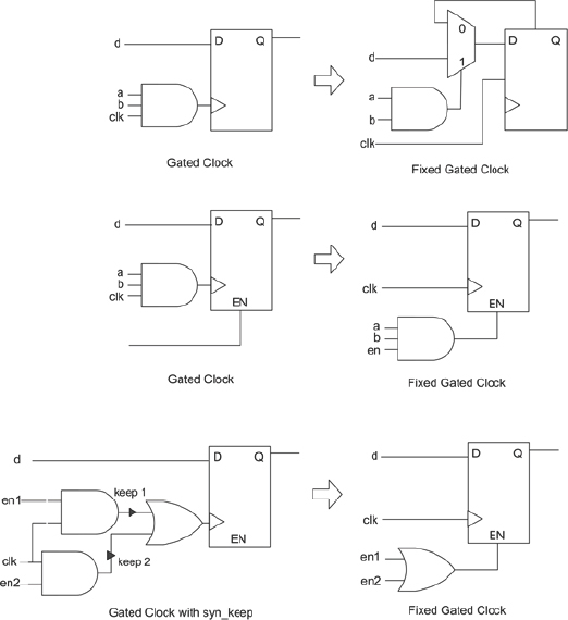
One function of synthesis beyond mapping to FPGA resources is the ability to manipulate the design automatically in order to avoid RTL changes. The most significant example of this is the removal of clock gating in the SoC design in order to simplify the mapping to FPGA.
Clock gating is common in SoC designs but is not a good choice for FPGA technology where dedicated low-skew clock distribution nets deliver un-gated clock to all registers on the die. Instead of gating clocks found in the RTL, the Synopsys Synplify® tool removes the combinatorial gating from the clock nets and applies the gating logic to the clock enable pin available on most sequential elements in the FPGA.
Figure 28 shows a few examples of clock-gating translations but there will be much more description of the manipulation of gated clocks in chapter 7. Synthesis needs to be guided in which clocks to preserve, how sequential elements, including RAMs, can handle clock enables and even how black-box items can be manipulated. This is all achieved without altering the RTL.
The resulting implementation after clock gate removal is logically equivalent to the input logic, but is more resource efficient and virtually eliminates setup and hold time violations due to the low skew clock distribution.
Finally, the synthesis is only part of the flow and an important consideration is how well the synthesis can collaborate with the other parts of the flow, particularly the place & route back-end in order to ensure that all tools work towards common goals. Let’s look now at the important subject of tools that perform design partitioning.
Figure 28: Examples of gated-clock removal performed by synthesis.
3.4. Design partitioning flows
Even though FPGA capacity has increased in line with Moore’s Law, the SoC designs themselves have also increased in size and complexity so SoC designs are still usually larger than today’s largest FPGA devices. As a result, the first law of prototyping is as true now as it was when first proposed at the start of the millennium and the prototyper is faced with the task of partitioning the SoC design into multiple, smaller FPGA devices.
There are two main approaches to partitioning: pre-synthesis or post-synthesis. We will consider each in turn here along with a less common approach of partitioning the actual SoC netlist.
3.4.1. Pre-synthesis partitioning flow
When the partitioning is performed on the design before synthesis, the input format is the RTL of the SoC design. The partitioning task is a process of creating FPGA-sized sub-designs from the overall design tree and can be automated to some degree. Figure 29 shows the steps in a pre-synthesis partitioning tool flow.
Figure 29: Pre-synthesis partitioning flow
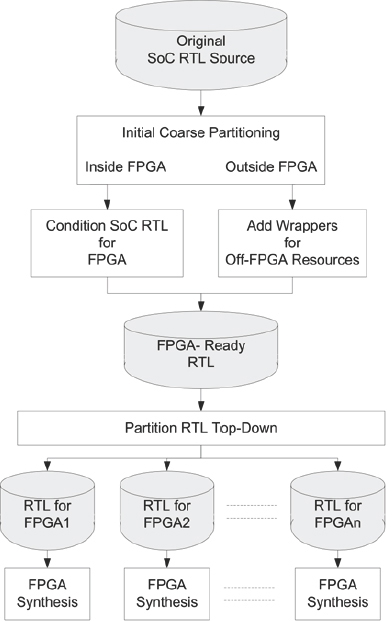
The flow is often performed top-down, which requires that the partitioning tools and the workstations upon which they run have the capacity to accommodate the whole SoC design, which can amount to gigabytes of data. Therefore, tool efficiency and runtime can become important factors and consideration needs to be given to the turn-around time from RTL changes to having a new version of the design partitioned and running on the prototype board.
Originally, the pre-synthesis partitioning approach dictated that compilation and synthesis occurred on the whole design, potentially resulting in long runtimes and demanding large server resources. However, recent advances mean that the FPGA synthesis is performed on all FPGAs in parallel. This requires that the partitioning makes an estimate of final results for each FPGA in order to infer timing budgets for the IO on each device. The benefit is that total runtime is greatly improved by running multiple synthesis tools in parallel. Turn-around time for each RTL change and bug fix is reduced accordingly, especially if incremental synthesis and place & route techniques are used. More detail of incremental flows is given in chapter 11.
The drawback of this flow is that it is actually a two-pass flow. To make a correct partition, some knowledge of final FPGA resources required by each RTL module is required. If possible, and if timing-driven partitioning is our aim, then a timing knowledge at each module boundary would also be useful. This accurate knowledge of resources and timing can only come from synthesis (or preferably from place & route). We therefore need to skip ahead and pre-run synthesis before feeding back the results to the partitioner. In the Certify® tool, that is precisely what is done. The synthesis is run in a quick-pass automated mode in order to estimate resources and timing. Thus, although a two-pass flow, the pre-synthesis in effect seems like an extra “estimate” step in a single-pass flow.
The case where top-down pre-synthesis partitioning can be most powerful is when performance, especially inter-FPGA performance, is crucial. By working top-down and using the system-level constraints, a pre-synthesis partitioning flow allows for timing to be budgeted and constrained across multiple FPGAs at the same time. The synthesis is also more able to account for board-level delays and pin-multiplexing in order to correctly constrain the individual FPGAs later in their respective flows.
3.4.2. Post-synthesis partitioning flow
As the name suggests, post-synthesis partitioning takes place after synthesis at the netlist level. Figure 30 shows how individual modules are synthesized and mapped into FPGA elements individually, resulting in numerous gate-level netlists. The netlists are combined into a hierarchy and then re-grouped into FPGA-sized partitions. At the same time, the netlists are conditioned for FPGA (e.g., gated clocks are changed to enables) and wrappers are created for modules which will be modeled externally (e.g., RAMs). We will discuss wrappers in detail in chapter 7.
The main advantage of post-synthesis partitioning is that only those RTL source files which have changed are re-synthesized, the results of the other RTL files being adopted without change. The resultant netlists are merged and the partitioning results are also likely to be reusable except in cases where module boundaries have altered. This lends itself to easier automation and scripting as a flow.
Figure 30: Post-synthesis partitioning flow
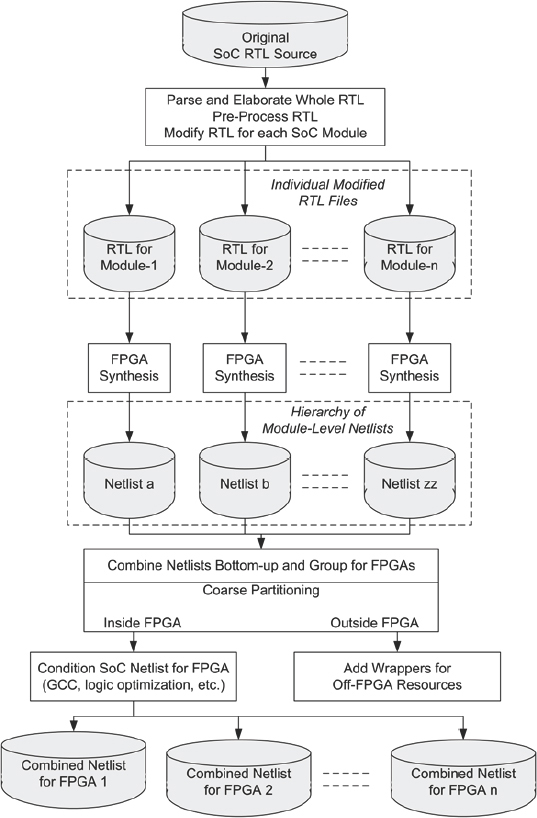
Another advantage of post-synthesis partitioning comes from the flow being a natural single-pass flow. That means that by the partitioning stage, the design is already mapped into FPGA resources and timing information is accurate enough to allow more accurate partitioning decisions. There is therefore no need for a pre-run on the synthesis in order to estimate resources.
Table 5: Comparing partitioning flows
| Pre-synthesis | Post-synthesis | |
| QoR | Best | Sub-optimal |
| Set-up | Top-down | Simpler |
| Turn-around | Needs incremental synthesis and place & route | Naturally block-based |
| Debug advantage | Multi-FPGA instrumentation | Name preservation |
| Full runtime | Slightly slower | Slightly faster |
Table 5 makes a short comparison between pre-synthesis and post-synthesis partitioning flows based on the discussions above.
The choices are between a faster turn-around time and more automation on the one hand, and best results on the other hand.
3.4.3. Alternative netlist-based partitioning flow
There are some teams that advocate an alternative flow for FPGA-based prototyping in which the synthesis is performed by the normal SoC synthesis tools and it is the resultant gate-level netlist, or hierarchy of netlists, that becomes the input for the rest of the flow. Figure 31 shows this netlist-level flow. Here we note that normal SoC synthesis is used and the design is mapped into the same cell library as for the final SoC. The task of mapping the design into FPGA elements is performed at a cell-by-cell level, via an intermediate format where the .lib cells are replaced with their functional equivalent. During the SoC synthesis, netlists may be manipulated using built in group and ungroup style commands to do the job of partitioning. The same top-level tasks still need to be performed as in the other partitioning flows i.e., objects unsuitable for FPGA implementation need to be isolated and doing this at a netlist level might be too complex for many users.
Figure 31: Alternative SoC netlist-based flow
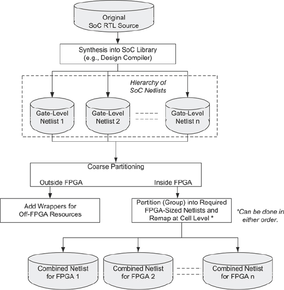
Nevertheless, netlist editors exist that allow very powerful manipulation of the design under the control of scripted netlist editor commands. Some find this preferable to changing RTL in order to do the same thing. We should understand that a netlist-based approach is likely to achieve lower performance and use more FPGA resources than the other flows because FPGA synthesis is limited to mapping a very fragmented design into FPGA low-level cells, missing many chances for optimization. All possibility of automatically inferring the high-level resources, such as DSP blocks or SRL functions of the logic elements from such a low-level netlist is lost.
We shall cover more about our uses of partitioning tools in chapter 8 but let us now move on from the front-end steps in our FPGA-based prototyping tool flow and consider the remaining steps in the flow that take our partitioned synthesized design into the FPGAs themselves.
3.4.4. Partitioning tool example: Certify®
Usually provided by third-party EDA vendors, these tools are used to automate and accelerate the partitioning of a single RTL code into multiple FPGAs. While partitioning can be done manually, for example by using group and ungroup commands and selective net-listing of subsets of the design, dedicated EDA tools significantly simplify and speed-up the initial partitioning and allow subsequent partitioning modification with ease.
Figure 32: Screenshot of Certify partitioning environment

Partitioning tools such as Synopsys’ Certify, pictured in Figure 32, perform a mix of automatic, interactive (drag-and-drop) or scripted partitioning. These kinds of tools allow what-if exploration of the partitioning options which is important because some designs will not appear to have obvious partition boundaries to begin with. Tools that allow quick trials and provide immediate visibility of utilization and connectivity can guide the users to better partitioning decisions than working completely manually at the netlist level.
For example, in the Certify screen shot we can see an interactive partitioning session is in progress. The top-level of the RTL is shown schematically in the centre panel. Here we see the core of the design and a simple chip-support block alongside, in this case just clock and reset (we shall explain more about top-level partitioning in chapter 8). At the top panel, we see a representation of the board resources into which we can partition. In this case, a simple board with two FPGAs, a RAM, external IO connectors and a clock source. On the left of this panel we can also see the board’s resources in a nested-list view, common to many EDA tools. In that list view and in the top-level diagram and other places we can see our progress as we assign various design elements to relevant board resources. We can also see other assignments into each FPGA, such as our debug instrumentation (in this case, Xilinx® ChipScope tools).
At each step, we get immediate feedback on how we are doing, for example, in this shot, the FPGAs have histograms showing proportion of logic, memory and IO used so far. Another useful guide for interactive partitioning is the connectivity matrix, showing the inter-block connections at this level of the design; this shot shows that there are 128 connections between the core of the design and the system-level interface (i.e., external IO).
Some further detail of the use of Certify tools, including pin multiplexing, fine-grain partitioning by logic replication and clock domain rationalization is given in chapter 7 and 8.
3.5. FPGA back-end (place & route) flow
Whether or not the pre-synthesis or post-synthesis partitioning is used, the results are a mapped netlist ready for each FPGA, plus the associated constraints for timing, pin-locations etc. At the end of the tool flow is a tool or rather a set of tools, provided by the FPGA vendors which can be considered the “back-end” of the flow, using common SoC terminology. These back-end tools take the netlist and constraints provided by the synthesis tools and implement the logic into the desired FPGAs.
A simplified flow diagram of the FPGA back-end is shown in Figure 33, where we see that the first step is to re-map this netlist into the most appropriate FPGA resources as optimally as possible. If synthesis has been correctly constrained and itself has good knowledge of the target FPGA technology then the netlist will need little remapping in the back-end.
The mapped resources are then placed into available blocks in the FPGA and routed together. The place & route runtime and results will depend on many factors, but mostly the quality of the constraints and the utilization of the device.
Figure 33: Xilinx place & route tool flow
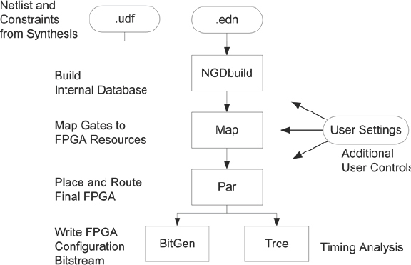
The final step is to generate the bitstream which will be programmed into the FPGA devices themselves (with RAM-based FPGAs such as the Xilinx® Virtex® families, we call this configuration rather than programming).
Throughout the back-end we can control and analyze the results of the various steps including timing analysis, floorplanning and even estimate the final power consumption.
These tools are generally available through a graphical design environment such as the Xilinx® Integrated Software Environment (ISE® tools) which is shown in Figure 34. Here we see the summary for a small design targeted at a Xilinx® Spartan®--3 device but the same approach is scalable up to the largest Xilinx® Virtex-6 FPGA, although the platform upon which the tool is run, especially the place & route tool, must be very much more capable. For this reason, most large prototyping projects run their tools on Linux-based workstations with maximum ram resources, which are generally widely available within SoC development labs.
Many users will run each of the above steps in an automatic flow, started by clicking a single “button” in ISE. However, it is also common to find that each step is launched individually with the appropriate arguments in a scripted flow or through a command-line interface. This allows unsupervised implementation of the FPGA in a semi-automated fashion which is beneficial when the runtime is many hours.
In that case, conditional branching or termination tests would be inserted at various points of the script to ensure that time is not wasted running tools after earlier steps had failed for any reason.
Figure 34: Xilinx® ISE® tools screenshot
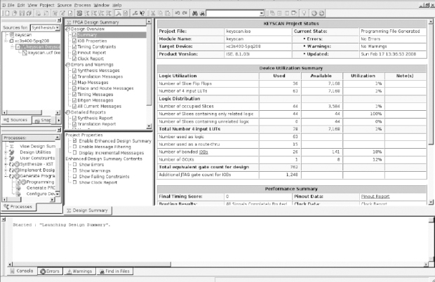
A useful way to get started with place & route scripts is to use the “generate script” command in the ISE Project Navigator. This generates a tool control language (TCL) script that contains all the necessary commands to create, modify, and implement the single-FPGA project from a TCL command prompt.
3.5.1. Controlling the back-end
At the top of Figure 33, we see alongside the edif netlist (.edn) a file called .ucf. This is the user constraints file (UCF) format file which is generated by synthesis and/or manually entered by the user and which is used to control the back-end flow.
The two most important parts of the UCF are the controls for constraining the timing and the placement of the back-end results. Here is where constraints such as clock periods, IO timing, RAM placement, logic grouping and even fine-grained logic placement can be enforced on the back-end. For a FPGA-based prototyping flow, the most useful part is the placement constraint for package pins. Figure 35 shows a short excerpt of a UCF which was automatically generated by a configuration tool for the HAPS® FPGA boards, called Hapsmap. This UCF is controlling some pin locations for a Xilinx® Virtex-5 FPGA on a HAPS-51 board and is setting their voltage levels to 3.3V. The UCF is also setting a control for one of the digital clock manager (DCM) blocks as well as defining some clock constraints using TIMESPEC commands understood by the Xilinx® back-end tools. There is more information about UCF in the references and we shall take a closer look at constraining FPGA designs during chapter 7 and chapter 8.
Figure 35: Example lines extracted from typical user constraints file (UCF)
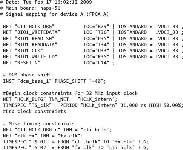
An important role for the UCF file is to act as a link between synthesis and the back-end in order to ensure that both tools are working towards the same goals. It is a common error amongst some FPGA designers to neglect the constraints for either part; for example, to provide only the most rudimentary clock constraints to the synthesis and but to then spend a great deal of time and effort tweaking controls for place & route in order to meet timing goals. Passing UCF forward from synthesis ensures that both synthesis and place & route play their part in optimizing the design and meeting design targets.
3.5.2. Additional back-end tools
Beyond the core flow outlined above, there are a number of other useful tools in the back-end suite which may increase our productivity during our prototyping projects. These additional tools include:
- Core generation: a tool which generates specially constructed and optimized design elements or IP cores. Such IP cores may be part of the original design or cores that may be used to replace special RTL structures with FPGA equivalent structures. Read in chapter 10 how we can use the Xilinx® CORE Generator™ to help with SoC IP prototyping.
- Floor planning: a tool that allows the user to create placement constraints to any design element. Typically used for IO placements but can also be used to place logic when performance is critical and the tools cannot meet performance requirements.
- Incremental implementation: tools that allow incremental design implementation only on parts of the design that were changed since the last run. Depending on the extent of changes, incremental implementation can significantly reduce the implementation time, compared to a complete re-implementation. Read more about incremental flows in chapter 11.
- FPGA editing: an editing tool that allows modification of the FPGA after place & route. Such tools (Xilinx® FPGA Editor) allow engineers to perform low-level editing of the design (more detail in debugging tools section below).
- In-circuit debugging: tools that allow capturing and viewing of internal design nodes. Debugging tools will probably be used more than any other in the flow and so we will consider them in more detail next.
3.6. Debugging tools
Some thought needs to be given to how the prototype is to be used in the lab. What debug or test tools will be needed in order to provide the necessary visibility? There are a number of tools which provide debugging capabilities such as access to the design’s internal nodes for probing, event triggers etc.
The debugging tools add some logic to the FPGA’s design that captures selected signals into unused memory blocks based on programmable events. After capture, the signals are read out from the FPGA using the JTAG utility and are displayed in a variety of ways such as waveforms or showing values in the source code. While some tools require the user to instantiate the capture logic in the RTL prior to synthesis, other tools add the instrumentation logic at the netlist level during the FPGA implementation phase leaving the RTL intact. In addition, some of the tools allow quick tool configuration changes without needing to go through the often lengthy place & route process.
3.6.1. Design instrumentation for probing and tracing
During the prototype bring-up process, often the design does not work right away and there is a need to diagnose its state and understand its behavior. Even after the initial bring-up, during active use of the working prototype, the design may exhibit unexpected behavior. In either case, the visibility provided by the FPGA and other component IO pins is not likely to be sufficient to properly debug the situation.
The prototype debug process requires visibility beyond that available only at the IO pins and this section describes common techniques that help instrument the FPGAs that comprise the FPGA-based prototype. We will also give an overview of some tools which can greatly aid the debug process and further tool detail is offered in the appendices.
Techniques for probing internal signals of a design implemented in FPGA fall into two general categories: real-time signal probing and non-real time trace capture.
3.6.2. Real-time signal probing: test points
Viewing nodes in real-time is a common debugging practice, as in addition to signals states, real-time probing can uncover race conditions and unexpected “runt” signals. In real-time probing, signals from the design are taken to bench instruments such as logic analyzer or an oscilloscope for design analysis. Probed signals are either normally available at FPGA boundaries, or specifically brought from the design’s internal nodes to FPGA test pins.
In this simplest method of probing designs’ internal nodes, the user directly modifies the design and brings internal nodes to FPGA pins for real-time probing. This method consumes little or no logic resources and only a few routing resources plus, of course, the actual IO pins that bring the probed signals to the outside world.
In general, the RTL would need to be altered in order to add test points to the design, so this may simply not be an option for many projects. However, some tools support the inference of test points without changing the code. For example, Synopsys FPGA synthesis tools support an attribute called syn_probe which will do exactly that.
If RTL changes do become necessary (and are allowed) then we should at least try to minimize the impact and scope of the changes. Thankfully, both major HDL languages support remote linking between different parts of a design hierarchy. This is achieved in VHDL using global signals and in Verilog-HDL using XMRs (cross module reference). More information and examples of using remote referencing is given in chapter 7.
One disadvantage of making RTL changes to bring out test points is the long turn-around time to view a different signal or set of signals. To view a new signal, the FPGA design RTL source would need to be modified and then the design is passed through the synthesis and place & route process. To mitigate this process, which might be rather long, it is recommended to consider in advance a superset of those signals that might be required for probing and bring as many to visibility points as possible. However, FPGA IO pins are a precious resource in most FPGA-based prototyping projects so the number of spare IO pins on the FPGA available to act as test points is likely to be low.
One simple and low-cost method for increasing the visibility into internal signals is to create in the design a “test header” port at the top-level to which we might connect the various signals and make changes with ease. To further minimize potential design spins or when the number of pins for signal viewing is limited, a slightly more sophisticated scheme where signals are multiplexed as shown in the following drawing:
Figure 36: Test pin muxing
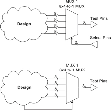
As shown in Figure 36, an eight-signal wide 4-to-1 multiplexer (MUX1) is added to the design and is statically controlled with two select bits from outside the FPGA. Such a multiplexer allows probing of eight signals at the time selected from a set of 32 signals.
A second eight-signal wide 4-to-1 multiplexer (MUX2) is shown but this is controlled by an internal processor or state-machine. This arrangement saves the two select pins and simplifies the multiplexer control in so me situations. If possible, we should use XMRs or global signals to connect lower-level signals for observation to the multiplexer inputs (more about the use of XMRs in chapter 7).
3.6.2.1. Note: probing using Xilinx® FPGA Editor
Another method of modifying the design quickly is to edit the design at the netlist level using FPGA tools such as the Xilinx® FPGA Editor. Using this tool the user can add design elements such as pins, and connect them to the nodes that need probing. It’s important to note that a tool such as Xilinx® FPGA Editor is very powerful but complicated to use and requires a very detailed knowledge of the FPGA’s resources. We therefore only recommend the use of Xilinx® FPGA Editor for experts only. There is further information in the references.
3.6.3. Real-time signal probing: non-embedded
This method of probing real-time signals is often provided as part of a commercial prototyping system, such as the CHIPit® systems from Synopsys, but could also be provided by in-house boards. The idea is to reserve a fixed number of pins from each FPGA and to route them on the board to a probing header, which acts as a debug port to which we can connect our logic analyzer. We can select the signals to be viewed on each FPGA, perhaps using a hierarchical design browser. The tool then directly modifies the already implemented FPGA netlist using one of the backend sub-tools called Xilinx® FPGA Editor, which then connects the desired signals to the probing header.
It takes only a short time to implement the connection from internal FPGA logic to the debug port. This is possible using a tool like Xilinx® FPGA Editor because we do not need to re-run synthesis or place & route.
Care should be taken with interpreting the information given with such an approach because it is possible that signals may take widely different times to reach the debug port from their sources inside the different FPGAs. As this is all taking place on a completely implemented FPGA, the signals must take whatever paths remain available inside the FPGAs. Therefore, some of these paths will be long and via non-optimal interconnect resources, especially if the FPGA utilization is high. As a result, the timing relationship observed between the signals will not necessarily represent the real relationship at the sources. However, it is possible to use Xilinx® FPGA Editor to measure the time delay of the path for any particular signal and then to use some logic analyzers to compensate for the known delay.
In a perfect environment, the design modification process and any timing compensation is transparent to the user but even in the lab, it is very useful to be able to quickly extract a signal and observe it on a scope.
3.6.4. Non real-time signal tracing
A shortcoming of direct FPGA signal probing is the limited number pins available for probing. A non real-time signal tracing uses a different probing mechanism and gets around this limitation. The non real-time design probing and debugging tools are available from FPGA and other EDA vendors. These tools comprise a mix of hardware and software, and provide a logic analyzer style capture in the FPGA where FPGA resources are used to implement and add to the design modules to monitor and capture a set of signals selected by the user.
Using the vendor’s software tools, the user then configures the trigger condition and capture type relative to the trigger condition. Leveraging the FPGA “read back” feature, in which each FF and embedded memory in the FPGA can be read through the JTAG port. The content of the captured signal values are then transferred from the capture buffer in the FPGA to the software application running on a host computer using the FPGA JTAG pod, usually the same one used to configure the FPGA in the first place. The capture buffer content can either be displayed on the vendor’s application or by other waveform display tools.
JTAG has some speed limitations, however, so some tools will make use of a faster FPGA configuration channel, if available. For example, Xilinx® devices have a facility called SelectMap which is used for fast parallel configuration. Synopsys’ CHIPit debug tools use SelectMap to quickly read back the captured register information in this way.
These tools are extremely useful for an individual FPGA debug, and in addition to their use as an “after the fact” analysis, some tools have ways to cross-trigger in order to synchronize external bench tools such as signal generators or software debuggers and this helps to correlate captured events across the system.
While there are a number of similar tools available in the market place, the most common FPGA probing tools for the Virtex FPGAs are the Xilinx® ChipScope series of tools from Xilinx and the Identify® tools from Synopsys and we shall give an overview of these in the following paragraphs before moving on to a debug strategy.
3.6.5. Signal tracing at netlist level
The ChipScope tool is an FPGA debugging tool from Xilinx for general purpose use, but with some special-purpose analysis versions available, for example for linking to embedded CPUs or analyzing fast serial IO. ChipScope tool works by adding extra instrumentation resources to the design in the device for the purpose of communication, triggering and trace capture. The instrumentation is synchronous to the design and uses the same system clocks as the logic being sampled, thus avoiding setup and hold issues. It should be noted that the trace capture is in actuality a sample of activity on an internal node of the FPGA. The timing resolution is of the trace data will be only the same as the capturing clock, therefore this is not a tool for analyzing absolute timing of internal signals.
Figure 37 describes the ChipScope tool implementation flow, showing two ways to add the instrumentation items to an FPGA design.
Of these two methods, the typical implementation flow is:
- Using Xilinx’s CORE Generator™ tool the user defines and generates the communication core and logic analysis cores to be embedded into the FPGA.
- The user then combines the cores with the FPGA design, either by instantiation into the RTL or directly into the synthesized design where the cores are merged at the netlist level so there is no need to modify the RTL design.
- Design must go through the synthesis place & route process before the tool is ready to be used.
The alternative is to insert the instrumentation at the netlist level:
- Use the ChipScope tool core inserter to open the netlist (either the edif from synthesis or Xilinx internal netlist, ngc).
- Select the clocks(s) and signals to be traced.
- The core inserter builds a new netlist and there is no need to use the CORE Generator™ tool.
- Pass results to place & route.
- In either case, once the instrumented design is downloaded into the FPGA, the use for debug is the same. The user communicates with the logic analysis cores via the FPGA’s JTAG download cable in order to set up the trigger conditions, capture mode etc. When the trigger and capture conditions are met, the tool transfers the captured data from the FPGA and displays it in the tool’s application running on the host PC.
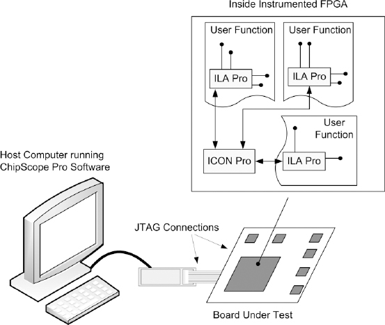
As shown in Figure 38, multiple ILAs can be instantiated in one FPGA while using only one communication core (ICON). An interesting feature available with ILA is the ability to generate a trigger output signal. This configurable signal reflects the trigger condition and can be routed to an FPGA pin and used to trigger other bench instruments. Although there is latency of ten clocks between the trigger event and the trigger output, it can be st ill used to correlate the trigger events with other parts of the system.
Figure 37: ChipScope tools design flow
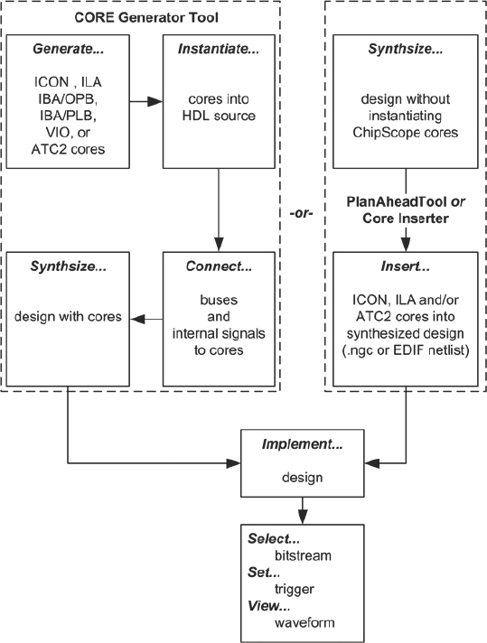
Figure 38: ChipScope™ Pro system block diagram
To view signals captured with LA1, Xilinx provides a custom graphical signal browser as part of the ChipScope™ software, a screenshot is shown in Figure 39.
Here we can see in the central horizontal panel an area for setting trigger values, which can be simple events or combinations of events over time using counters. There are two ways shown for viewing captured samples, one is showing a traditional logic analyzer style of view while the view to the bottom right is of the variation of a bus value over time, represented as an analog waveform. These signal viewers also allow a variety of features such as signal renaming, regrouping, reordering etc. so we are in a very familiar environment like a logic analyzer or scope, even though the “engine” of it all is embedded in the FPGA.
Figure 39: Screenshot of ChipScope™ debug tool
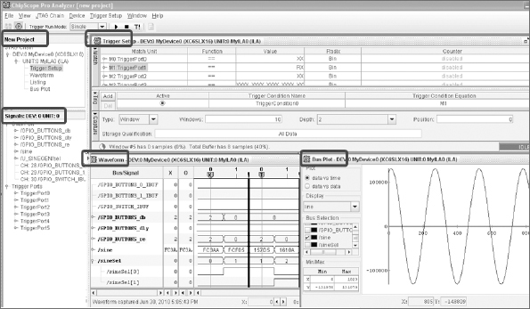
In addition to displaying captured data using the signal browser, ChipScope™ software can export the captured data in a variety of formats, including VCD (Value Change Dump), ASCII and Agilent’s FBDF (Fast Binary Data Format). Exported data can then be further viewed or analyzed by user scripts or by a wide variety of third-party tools.
3.6.6. Signal tracing at RTL
Identify® is a tool supplied by Synopsys which works in a similar way to the Xilinx® ChipScope tool except that instrumentation takes place at the source RTL rather than at the netlist level. Like ChipScope software, Identify instruments the design by the inclusion of signal monitoring logic, trace capture and buffering, and communications to a host PC. In addition, Identify tools provide signal select ion and monitoring mechanisms which enable the user to more easily trigger the trace capture and to correlate the captured information back to the source RTL.
Identify tool is comprised of two sub-tools, called the RTL Instrumentor and the RTL Debugger: The key part of the instrumentation logic itself is called an IICE (pronounced “eye-ice”) or intelligent in-circuit emulator, which is embedded into the user’s design. The IICE contains the probing logic, the trigger logic and trace buffers plus the runtime communication to the host running the RTL debugger.
Figure 40 gives an overview of the concept behind an RTL debugger. This is actually a screen shot and block diagram of the Synopsys Identify tool in its basic configuration. The tool inserts an IICE probing block that samples internal node information and gathers it together into a sample buffer, generally using one or more of the available FPGA BlockRAMs.
Figure 40: Synopsys Identify® tool overview
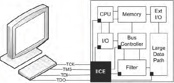
The IICE also includes triggering and sequencing logic for deciding when samples are captured. The IICE communicates over JTAG to the application where breakpoints and the state of the captured signals are shown and highlighted in the design’s RTL source.
Figure 41 describes the general usage flow for Identify, showing a two-pass strategy to focus in quickly to “zoom in” on data required for a specific debug task. As shown in the left process (first pass), Identify cores are added to the design before synthesis, followed with the place & route processes, but subsequent changes (second pass) to the instrumented signals are implemented incrementally where the synthesis and place & route steps are by-passed.
Figure 41: Identify use model and flow
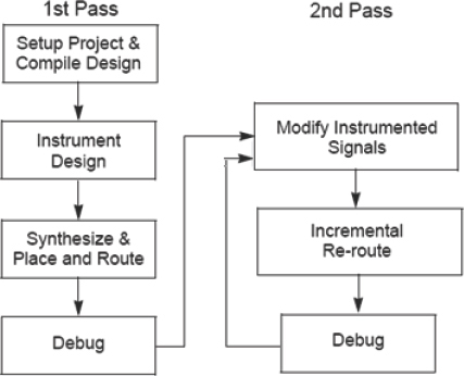
The following describes in more detail Identify’s main usage flow:
- Using Identify’s Instrumentor, the user selects signals to monitor and trigger conditions directly in the design from a hierarchical RTL source viewer.
- Instrumentation automatically generates the IICE core.
- After synthesis and place & route, the IICE core is controlled by the Identify Debugger where the user sets the trigger condition and arms and monitors the running hardware via the FPGA JTAG facility.
- After trigger, data captured in FPGA memory is uploaded to the Identify Debugger application software over the FPGA JTAG facility.
- Captured data can be displayed in a variety of ways: either directly annotated into the RTL code, or using common third-party waveform viewing tools.
- Small changes to the signal list and trigger conditions can be quickly made incrementally without going through the synthesize place and route processes.
A design can contain multiple IICEs, each configured in different clock domains and allowing different trace and trigger conditions. IICEs can cross-trigger between themselves so as to track a complex sequence of events. Multiple IICEs in an FPGA share the same communication mechanism with the JTAG interface.
In addition, the IICE provides the option of exporting the trigger condition, where a copy of the trigger signal is brought to the design top level and used to sync to bench instruments or software debuggers for enhanced system-level debugging. Linking to a software debugger is covered in more detail in chapter 11.
The Identify RTL Instrumentor is a sub-tool running on the host by which the user browses the design RTL in order to select the signals to be traced and if desired added to various cones of trigger logic. During instrumentation, the IICE is configured and added. The most useful aspect of making such instrumentation at the RTL is that we can easily keep track of what visibility we are adding. Figure 42 is an excerpt from an Identify screen shot which shows the RTL source code appears during an instrumentation process. The available signals for sampling are underlined and the cartoon spectacles change color if that signal is sampled, or part of the trigger logic, or both. The sphere icons on the left show where breakpoints might be inserted adding a useful feature to allow us to trap when the design reaches a certain line of code in much the same way as software engineers might debug their code.
Figure 42: RTL Instrumentor source code view

Let us now look at the in-lab debugger part of Identify. The RTL Debugger is the sub-tool that provides an interactive interface that we use in the lab to control the triggering, capture, and various flow-control features such as breakpoints. The debugger also provides the interface to waveform viewers.
Like ChipScope software, the Identify debugger provides a number ways to view the captured sample data and signals including:
- State annotation: when using break points, it annotates the signals’ state directly into the source code using the supplied design navigator tool. Figure 43 shows a screen shot of Identify RTL Debugger displaying the RTL source annotated with breakpoints and captured data states. In reality, the captured data is overlaid on the source code, highlighted in yellow and users can scroll through sampled data and see the values on the source code screen change. This is roughly analogous to the stepping through a software debugging tool.
- Waveforms: in addition to state annotation, Identify Debugger can interface with popular waveform viewers such as the freeware GTKWave viewer or the DVE environment provided with Synopsys simulators. The trace samples can also dump the signals into a standard VCD (Value Change Dump) file that can also be displayed on a wide variety of available waveform viewers.
Figure 43: RTL debugger source code view showing sampled data
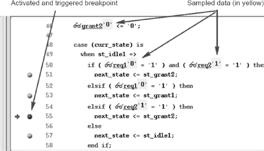
FPGA resources used by Identify consist of the capture logic and the capture buffer that is usually implemented in on FPGA BlockRAM. The size of the analysis resources depend on the number of signals to be captured, the trigger condition and to a greater extent, the desired capture buffer depth.
3.6.7. Summarizing debugging tool options
One of the traditional complaints against FPGA-based prototyping was that visibility into the design once inside FPGAs was very poor and that debug was non-intuitive because even when we had visibility, we didn’t really know what we were seeing. After this section, we have seen many different ways to add debug visibility into our prototype and there are many other tools available which are variations on the instrumentation approach taken by Identify and ChipScope software. We have summarized the approaches in Table 6.
Table 6: Comparing debugging technique and tools explored in this chapter
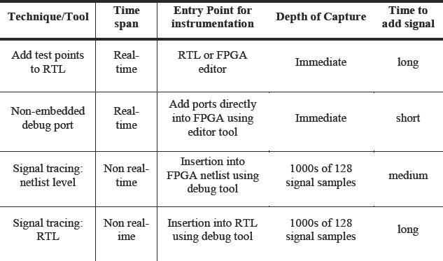
3.7. Summary
In this chapter we have aimed to give an overview of FPGA devices and tools today from our unique prototyper’s perspective. We described the main features of FPGAs themselves with specific reference to Xilinx® Virtex-6 family, discovering that the usefulness of each FPGA feature depends not only on its functionality but also on its support by the relevant EDA tools.
Regarding the EDA tools, we considered the need to address the so-called “three laws of prototyping” and the tools that enable us to do that, including synthesis, partitioning and place & route.
There are many more details available in our references but, now that we have a good understanding of the FPGA technologies involved, in the next chapter we shall get started in our FPGA-based prototyping project.
The authors gratefully acknowledge significant contribution to this chapter from
Joe Marceno of Synopsys, Mountain View