Verilog Simulation
To test the design I used ModelSim XE (with the free "starter" license that comes with the WebPACK). The project navigator will automatically build you a skeleton test harness based on your main project file. All I did was add 15ns wire delays for pretty display and then hand-coded a few transactions from the bus master's perspective. I wasn't ambitious enough to automate the testing — I just examined the output in the waveform viewer.
The following examples all show the core synthesized with "fast" DEVSEL# timing. The address and command are decoded during the address cycle and DEVSEL# is asserted immediately on the next cycle.
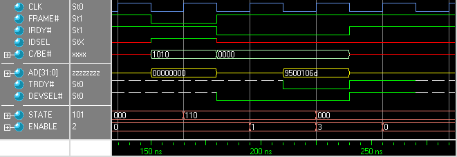
1010 Configuration Read
The first transaction any PCI target is likely to see is a read of the configuration space. Here's an example of a read of the DWORD at address 0x0 of the config space. The master asserts FRAME# and the target's IDSEL line along with the config read command 1010. The target only decodes AD[7:2] (in practice IDSEL is multiplexed with one of the upper address lines and is only defined to be valid during configuration transactions).
After the address cycle there is a mandatory turnaround as the master quits driving AD and hands them over to the target. The master immediately starts driving the byte enables on BE#. If the target could save some effort, or if there were side-effects for reading certain bytes, it could decode the byte enables to determine which byte lanes had to be valid. In our case the target can ignore the BE# lines and provide all 32 bits.
The CPLD doesn't have to do a lot of work to decode the address cycle, so it identifies itself as the target with DEVSEL# right away. It can't do anything else on that turnaround cycle, but on the next cycle it provides data on AD and signals that it is valid by asserting TRDY#. Since the master is not asserting FRAME# during this data phase it is the last one, and all that is left is for the target to drive DEVSEL# and TRDY# high for one clock to get the bus back into the idle state.

1010 Configuration Write
The write case is has an identical address cycle. There's no need for a turnaround cycle because the master retains ownership of AD for the entire transaction. Here we see a write to the config space at offset 0x4. It is setting a bit in the command register.
Memory space reads and writes have the same structure but use the MEMREAD and MEMWRITE commands and rely on the devices on the bus to decode all of AD to know if they are being targeted, rather than using IDSEL.

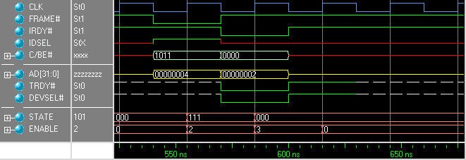
Burst Read
Here's an example of a burst read with a wait cycle inserted by the master. The burst is indicated by FRAME# remaining asserted through the first data phase. As long as FRAME# remains asserted the master expects at least one more data phase (there are ways for the target to abort which we don't need or implement). The target then provides the next DWORD of data and properly sustains it through a wait state indicated by IRDY# being deasserted by the master.
Bonus points if you spot the error in the sample data...

Other Transactions
The target also handles fast back-to-back transactions (where the next address phase happens immediately when DEVSEL# is de-asserted) and longer bursts.
The only other thing the target has to worry about is other targets' transactions. When it ignores a command it waits for FRAME# to de-assert (it can never be re-asserted in the same transaction) and then goes back to looking for address cycles.
And Then a Miracle Occurs...
After simulating my original design and programming the CPLD while the card was in the sacrificial "smoke test" motherboard I was able to boot with it in another PC and read/write it on the first try. You could have knocked me over with a feather. This turned out to be fantastically lucky, since when I went back to re-write my design more cleanly I made a silly mistake that broke it. When I booted with it I discovered that the BIOS/Chipset combination in the motherboard disables CLK if you don't respond to config cycles. It took me long enough to realize that was what was wrong that if I hadn't seen it work the first time I would have assumed that I had botched the board or the CPLD was too slow (being the slowest speed grade and in fact way, way out of spec for PCI).
Simulation is your friend.