The What and Why
Arbitrary Waveform Generator with a USB and PCI interface.
I have used FPGAs at work in the past , but wanted to get a little more experience using them and learn how to interface with the PCI and USB busses. I decided to create an arbitrary waveform generator as it is a relatively simple device and very useful for testing other circuits. An arbitrary waveform generator is a very flexible function generator. Memory is loaded with a series of values, and the hardware runs through the memory converting each value to a voltage at the output. This is the same as repeatedly playing a sound file on a PC, only potentially much faster. This card has a memory buffer that will hold 512K samples, and will run at a sample rate between .01Hz and 16MHz. Sample rates up to 50MHz are possible if the resolution or memory depth are reduced. The output voltage range is +/- 2 volts into a 50 ohm matched load.
Here's the output for a couple of signals: An ordinary sine wave, and the letter A.
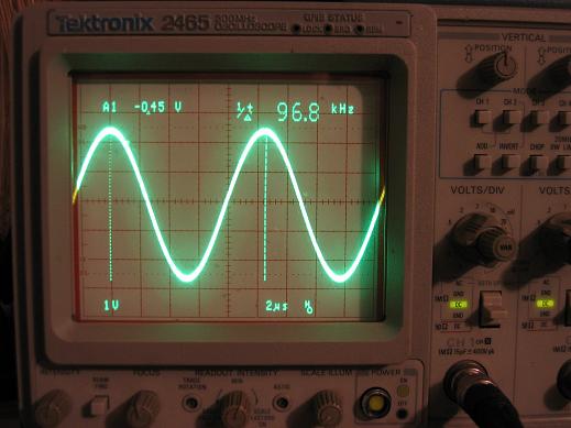
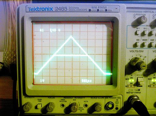
Below are block diagrams for the board and for the internal structure of the FPGA.
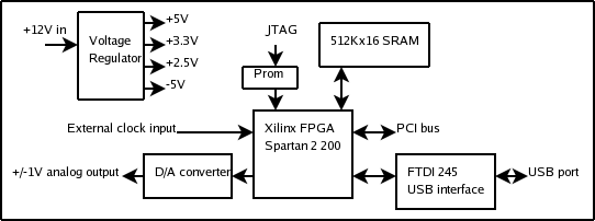
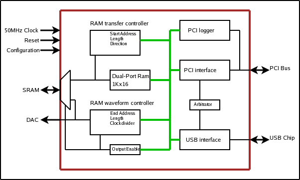
Tools and Help:
The PCB was designed using the Schematic capture and PCB layout tools from expresspcb.com
The FPGA code was synthesized and simulated with the Xilinx ISE and Modelsim packages, available from Xilinx.
The code for the PCI interface was taken from another hobbyist Ben Jackson at http://www.ben.com/minipci/.
Application and driver code were written in C using MS Visual C 4 under Windows and gcc under Linux.
The driver code is based off of information and examples from Linux Device Drivers.
I used PCI&PCI-X Hardware and Software by Solari and Willse. as a reference for the PCI bus, but hesitate to recommend it as it is more of a technical reference than a howto, the mechanical drawings don't quite match modern cards and the binding fell apart the first day I used it.
I did all my development on a single PC: the PCB design, FPGA code, and serial port control under Windows, and then ported the serial port control to Linux and developed the PCI driver under Linux. Having two PCs; either Windows and Linux or both Linux would have saved a lot of rebooting when debugging the PCI interface.
Hardware Design:
The Schematic and Layout files are here. Note that there are some errors with the design and symbols that are described in the mistakes.txt file.
The tools I used don't have any of the error checking that most other tools have, but they're free and the boards produced are cheap. There are a couple of hitches: there is no way to split power planes, and the minimum outline radius is greater than the slot size of the PCI connector. I marked the slot positions with traces, and used a dremel cut-off wheel to cut the slots.
When I created the PCB, I wasn't sure which PCI signals were necessary, and I included too many. The DAC also uses too many lines. I designed the board with a 16-bit part in mind, but that was not available so I used the 12-bit version instead. With the noise from a common digital and analog ground plane, it is unlikely that the difference in resolution matters. The SRAM chip on one of my boards had bad address lines on data bits 5 and 6, so I swapped the lines with bits 0 and 1 in the .UCF pinout file. For real fun and games, replace the SRAM with DRAM.
Schematic pages:
FPGA
FPGA support
DAC and USB
PCI and SRAM
Power
Here's the Finished board:
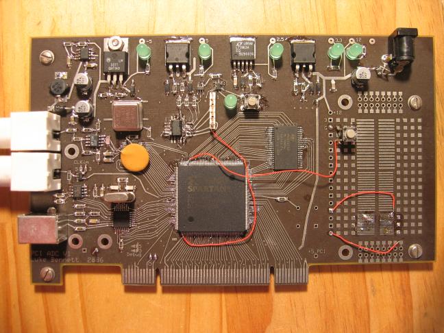
The output is one of the BNC connectors on the left side of the card, and the USB connector is below it. The card edge connector fits in a USB expansion connector as a 5/3.3V universal device. External power can be connected to the jack on the top right of the board.
The total cost was around $500 for two cards. The PCB cost $200 for a pair (minimum order) and the components around $300. It should be possible to reduce the cost by up to $100 with simple changes to component selection.
FPGA design:
All the code is written in Verilog. The module simulation_level is the top-level simulation module, and fpga_top_level is the module that should be synthesized to generate the FPGA configuration. The RAMB4_Sx_Sx_modified.v files are copied from the Xilinx package, but modified to not use the global reset line in the FPGA. The RAMB4 files must be included in the Modelsim project, but should not be included in the ISE synthesis project.
The FPGA design is centered around an internal buswith 16 data and 11 address lines. The bus is syncronous, with the clock line driven by the current master. The only non-obvious part of the bus operation is in a read operation: the peripherals respond to the address in the clock cycle before the read line is asserted. This is how the internal block ram operates, and the other registers emulate this behavior for consistency.
The dacdriver module does not allow direct access to the external SRAM, as it is far too slow for the PCI bus. Instead, data is written to a 1K word internal ram, and a state machine loads the data from the internal buffer to the external SRAM.
The USB interface is a state machine that listens for incoming characters on the USB port, then reads or writes data on the internal bus, and sends any read data back on the USB port. The packet format for the interface has a 20 bit address field, which is leftover from when it could directly access the external SRAM.
Here are the FPGA source files:
simulation_level.v
	pci_emulator.v
	sram_emulator.v
	usb_emulator.v
	fpga_top_level.v
		fpga_top_level.ucf
		analyzer.v
		arbitrator.v
		dacdriver.v
		debouncer.v
		pci_interface.v
		usb_interface.v
USB driver code:
The USB port looks just like a serial port to the application software. In Windows, the VCP drivers from FTDI for the 245 chip must be installed, and the port will get a COMx designation. In Linux, the drivers are already included in the 2.6 kernel, and the device is controlled through /dev/TTYUSBx.
PCI driver code:
The PCI port is currently only accessible under Linux. The driver I wrote is horribly inefficient, but it works. All the driver code is written in C. To compile the driver code, you must be running a Version 2.6 Kernel that has been compiled with the source tree installed. I am running Fedora Core 5, which required installing the kernel-source rpm and recompiling the kernel. To compile the driver module, run make from the driver source directory. The load and unload script in the same directory will load and unload the module, and also deal with linking the driver module to the appropriate /dev file. load and unload must both be run as root, but the /dev file is given wide open permissions in order to allow a regular user to run the application.
Tools for writing Windows PCI drivers are available, but beyond my budget.
The entire driver code is in pci_arb.c The functions are called at various times by the kernel pci_arb_init() pci_arb_exit() are called when the module is loaded and unloaded. These functions register all the other functions with the kernel. After the module is loaded, an associated /dev/ file is created (in the "load" script) which application code will use to access the device. arb_llseek(), arb_read(),arb_write(), arb_ioctl(), arb_open(), and arb_release() are called when application code calls corresponding functions on the /dev/ file.
probe() and remove() are called from the pci controller and are used to initialize the device and manage the memory space that is used to communicate with the device.
User Application:
The application has three different versions. A Windows and a Linux application that commuunicate with the card over USB, and a Linux application that communicates over PCI. There is a common file called sa_portable.c that contains the main program, and three different files that handle communication: linux_arb_pci.c, linux_arb_usb.c, and windows_arb_usb.c. os_arb_interface.h contains the function prototypes for the three communication files. The different applications are created by the choice of communication file linked in.
To built the Linux applications, run make from the application_code directory. sas is the USB executable which must be run as root, and sap is the PCI executable which can be run as a normal user.
I did not include a project for a Windows build. Just create a regular console application project and add sa_portable.c and windows_arb_usb.c.
To generate the A image at at the top of the page, load the file sample.waveform. The file format for the waveform is a character specifying the radix of all the numbers in the file -x for hexadecimal, anything else for decimal- followed by a number specifying the length of the waveform, followed by the values for the samples.
Performance:
The sample clock on the card is 50MHz, which corresponds to the maximum sample rate of the DAC. unfortunately I couldn't find any big, fast, cheap SRAM chips, so the output sample rate is limited to 16.6MHz. running at 25MHz, there are a few glitches, and at 50MHz there are many. The sample rate could be increased by packing in two samples per memory word limiting resolution to 8 bits or changing to a grey code counting scheme which would limit waveform lengths to powers of two.
The output is limited by the +/-5V supply rails which cause the amplifier to clip at +/-1/4 full scale, turning the 12-bit converter into a 10-bit converter. I should have used a lower gain amplifier than the one specified on the DAC reference design, as changing the gain on this one will be hard without either making it unstable or ruining the slew rate.
The communication between the PC and the device does not make efficient use of the interface, but as I will rarely be transferring large amounts of data, there is no real need to improve it. Improving the speed of both USB and PCI could be done by transferring blocks of data, instead of one word at a time.