Objective
The purpose of this task was to analyze the design of the FPGA-based, MSE / MAD Classifier board utilizing Omniview's Cosmos performance modeling tool suite. The goal of the performance modeling activity was to determine:- the number of FPGA-based custom boards required to meet the MSE Classifier throughput requirements
- the complexity level required for the board control processor
- the partitioning, distribution and granularity of the processing load for the low- and high-resolution MSE processing, and
- the on-board memory requirements.
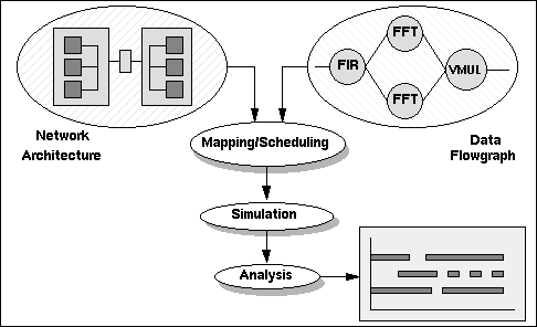
Cosmos performance models are made up of two major components: a hardware model (network architecture) and a software model (data flowgraph). The hardware and software models are defined independently and to the same level of detail. The independence of the models ensures a hardware architecture can be utilized with various software architectures and vice versa. Modeling both hardware and software at the same level of abstraction ensures that high-fidelity performance models are created and prevents hardware or software from dominating the model. Figure 1 shows how Cosmos' independent hardware and software models are merged, simulated and analyzed as a result of the mapping.
The following low resolution parameters from the test and template data and were used to parameterize the Cosmos performance model:
In this case, the high resolution parameters derived from the test and template data analysis and used to define the Cosmos performance model:
To simplify the development effort while ensuring the integrity of the performance model, the following elements were modeled:
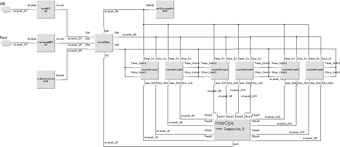
Cosmos' Hardware Designer enables engineers to capture hardware architectures hierarchically. Figure 3 shows the top-level hardware architecture performance model represented in Cosmos. Previously, Cosmos had predominately been used to model multi-processor systems. However, with only minor adaptations, it was successfully used to rapidly model the SAIP MSE FPGA custom board design.
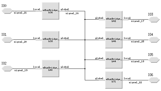
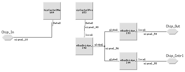
To accurately capture the behavior of each of the hardware elements, several techniques were developed. The PML library was limited in terms of the number and variety of hardware elements that it supported. For example, the PML library did not support a local "multi-drop" bus structure that is fairly common among board designs. However, standard PML hardware elements were used and adapted to accurately model the desired behavior. For instance, the VME bus bridge library element was used to model the behavior of the "multi-drop" bus. Figure 4 shows how the PML VME bus bridge library elements were adapted and combined to create the local "multi-drop" bus model.
In addition, processor elements were used to model the various memory and storage devices. This was accomplished by devising an approach, as shown in Figure 5, to accurately model the behavior of a dual-ported memory device. Two processor elements were configured in a manner to properly model the behavior of a dual-ported memory device. One processor element was used to model the input port of the device while the other processor was used to model the output port. Using this approach, tokens could be written and read from the device model simultaneously.
Cosmos automatically generates token routing tables based on specifying a software task as the token's destination. A token routing table is a static "lookup" table that defines all of the possible software communication paths throughout the system. This was the primary reason all of the hardware elements, including memory and storage devices, were modeled as processor elements. Using this approach, the communication task could be mapped to the memory and communication elements as software tasks.
The flow of commands and data through the system was very structured and processing flows were divided into two modes, Low and High Resolution. The tables below show, in detail, the flow of commands and data for the low and high resolution modes.
Step
Source
Destination Message Name Size 1. Board Controller Ext. Template Data Storage Load Template Data 1 Kb 2. Ext. Template Data Storage Int. Template Data Storage Template Data 18 Mb 3. Int. Template Data Storage Board Controller Load Complete 1 Kb 4. Board Controller Int. Template Data Storage Fetch LR Template 1 Kb 5. Int. Template Data Storage Template Cache In 1
LR Template Data 6240 bytes 6. Board Controller Ext. Chip Data Source Fetch LR Chip 1 Kb 7. Ext. Chip Data Source Chip Cache In (6) LR Chip Data 2916 bytes 8. Board Controller Chip Cache Out (6) Fetch LR Chip 1 Kb 9. Chip Cache Out (6) MSE / MAD Operator (6) LR Chip Data 2916 bytes 10. Board Controller Template Cache Out 1
Fetch LR Template 1 Kb 11. Template Cache Out 1
MSE / MAD Operator 1 LR Template Data 6240 bytes 12. 13. MSE / MAD Operator 6 Board Controller Load LR Template 1 Kb 14. Board Controller Int. Template Data Storage Fetch LR Template 1 Kb 15. Int. Template Data Storage Template Cache In 1
LR Template Data 6240 bytes 16. Repeat for all 20 Target Classes - Go to Step 10
Step Source
Destination Message Name Size 1. MSE / MAD Operator 6 Board Controller Load HR Chip 1 Kb 2. Board Controller Ext. Chip Data Storage Fetch HR Chip 1 Kb 3. Ext. Chip Data Source Chip Cache In (6) HR Chip Data 5202 bytes 4. Board Controller Chip Cache Out (6) Fetch HR Chip 1 Kb 5. Chip Cache Out (6) MSE / MAD Operator (6) HR Chip Data 5202 bytes 6. MSE / MAD Operator 6 Board Controller Load HR Template 1 Kb 7. Board Controller Int. Template Data Storage Fetch HR Template 1 Kb 8. Int. Template Data Storage Template Cache In 1
HR Template Data 49200 bytes 9. Board Controller Template Cache Out 1
Fetch HR Template 1 Kb 10. Template Cache Out 1
MSE / MAD Operator 1
HR Template Data 49200 bytes 11. Process Data, 4.908 ms 12. Go to Step 4 - Low Resolution Processing
Approach
The FPGA based MSE/MAD performance modeling effort was accomplished using Omniview's Cosmos tools and performance modeling library (PML). Cosmos facilitates the rapid creation of high-fidelity performance models of multi-processor systems. The models can be used to quickly perform trade-off analyses of candidate hardware and software architectures. Cosmos facilitates determining whether a design will satisfy the performance requirements, identifying bottlenecks and optimizing a system's performance.
Processing Requirements
The MSE /MAD classifier function determines which set of targets, in a target template database, best matches the current image chip. In the first stage, comparisons are performed on a low resolution image chip. Incoming image chips are evaluated against 20 target classes, each having 72 different pose angles and 121 offset locations. In the second stage, the top five low resolution target classes are used to determine the best high resolution match based on a limited number of pose angles and offset locations. The system specification requires that the MSE Classifier process at least 30 image chips per second. The following sections describe in detail the specific requirements of the low and high resolution modes. Low Resolution
The low resolution processing requirements are as follows:
High Resolution
The high resolution processing requirements are as follows:
Hardware Architecture Implementation
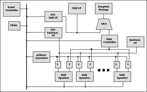
A graphical representation of the FPGA-based MSE Classifier custom board is shown below (see Figure 2). The classifier was made up of six FPGAs each accompanied by dual-ported template and chip caches, external VME and RACEway interfaces, a board control processor for dispatching the image chips, and global template memory to store the target templates for both the low and high resolution modes.
Software Processing Flow Implementation
Cosmos' Software Designer enables engineers to capture the inter-task communications and define the lower level software descriptions using data flow graphs. To facilitate the MSE FPGA custom board model development, software tasks were used to mechanize the routing tokens throughout the model. As a result, unique software tasks had to be allocated for each processor element defined in the hardware architecture. Figure 6 shows the top-level software description in which all of the software tasks are defined including the inter-task communication paths.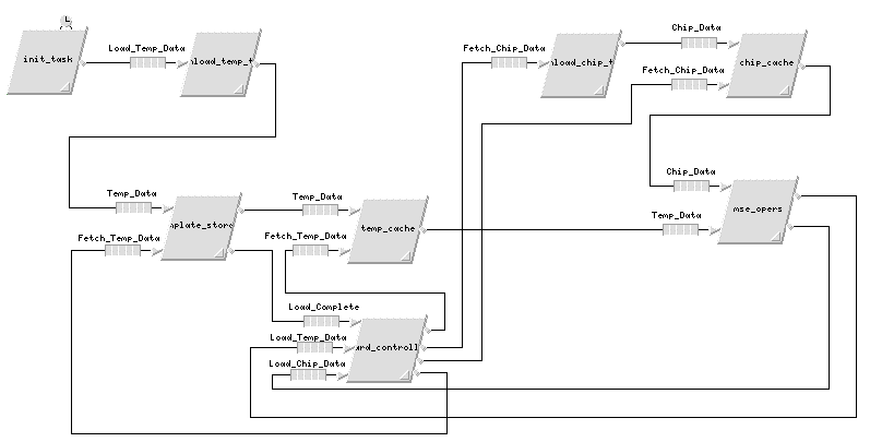
Template Cache In 2
Template Cache In 3
Template Cache In 4
Template Cache In 5
Template Cache In 6
Template Cache Out 2
Template Cache Out 3
Template Cache Out 4
Template Cache Out 5
Template Cache Out 6
Template Cache Out 2
Template Cache Out 3
Template Cache Out 4
Template Cache Out 5
Template Cache Out 6
MSE / MAD Operator 2
MSE / MAD Operator 3
MSE / MAD Operator 4
MSE / MAD Operator 5
MSE / MAD Operator 6
Process Data, 2.04 ms
Template Cache In 2
Template Cache In 3
Template Cache In 4
Template Cache In 5
Template Cache In 6
Template Cache In 2
Template Cache In 3
Template Cache In 4
Template Cache In 5
Template Cache In 6
Template Cache Out 2
Template Cache Out 3
Template Cache Out 4
Template Cache Out 5
Template Cache Out 6
Template Cache Out 2
Template Cache Out 3
Template Cache Out 4
Template Cache Out 5
Template Cache Out 6
MSE / MAD Operator 2
MSE / MAD Operator 3
MSE / MAD Operator 4
MSE / MAD Operator 5
MSE / MAD Operator 6
Simulation Results
Cosmos provides the capability to import VHDL simulation transcript files to visualize the processor activity as a function of time. Analysis of the simulation results (see Figure 7) show it took 57 milliseconds to process one image chip for both the low and high resolution classification modes. As a result, a single board can process 17.5 image chips per second and two FPGA-based MSE/MAD Classifier boards would be needed to process the required 30 image chips per second. The processing throughput of the two board subsystem actually exceeds the system requirements by over 16 percent. It is appropriate to point out that the simulation results indicate that the FPGA-based MSE/MAD operators are inactive throughout the processing. This is attributed to the fact that the performance model's abstraction level is not down to the clock level, but rather at the block level.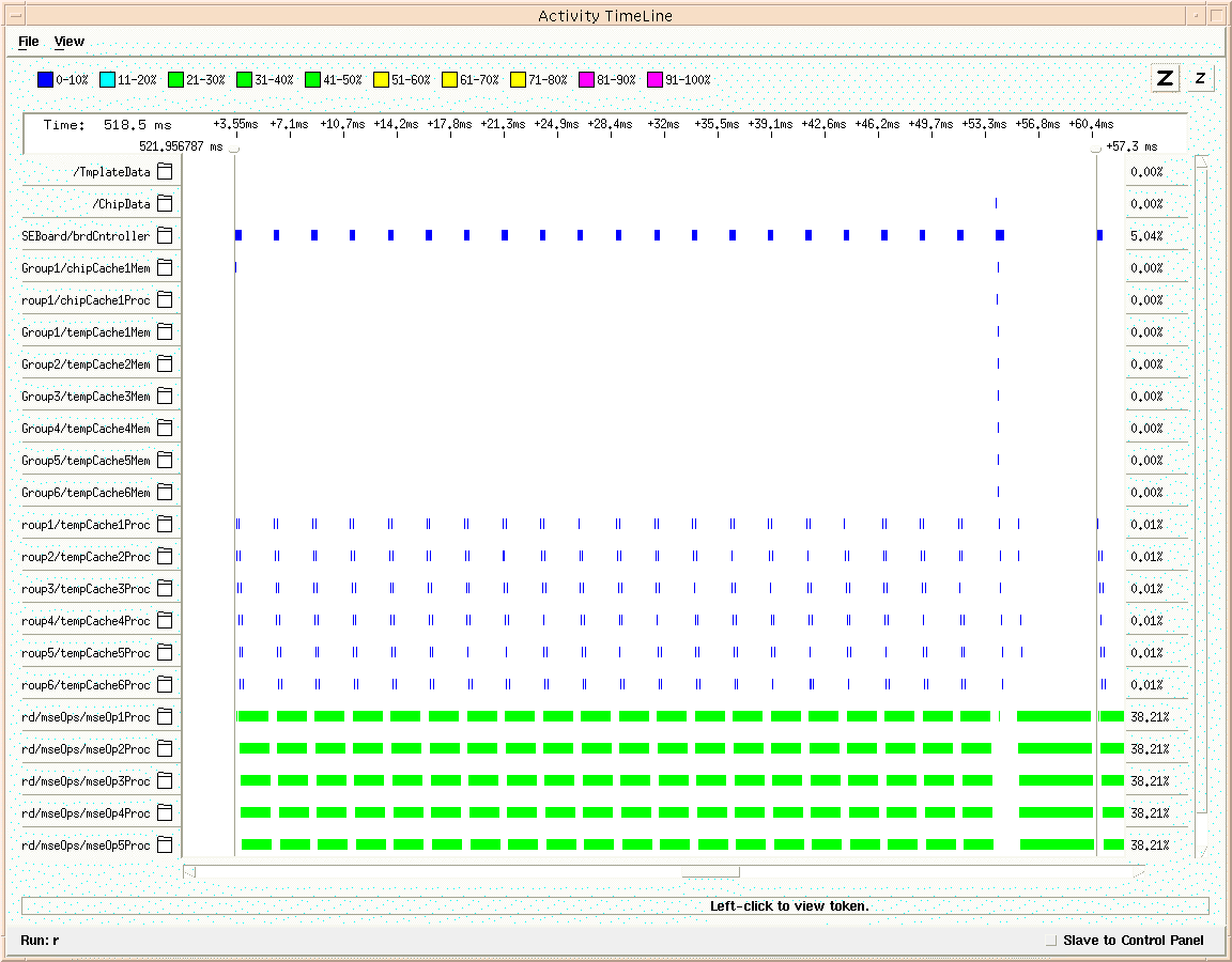
Summary
In summary, Cosmos was successfully used to model and analyze the MSE/MAD Classifier FPGA custom board hardware and software design. Techniques were devised to use Cosmos' existing library elements and adapt them to model the FPGA MSE operators, the image chip and template caches, the board controller, the template storage memory, and the VME and RACEway network interfaces. Results from this board level performance modeling effort verified the top level software architecture for the low and high resolution MSE processing functions and provided the timing estimates needed to establish the number of FPGA custom boards needed to meet the BM4 requirements. The results from this virtual prototyping effort combined with the results from the C80 and C6201 custom board performance modeling efforts provided the data needed to make the final BM4 MSE Custom Board architecture selection.