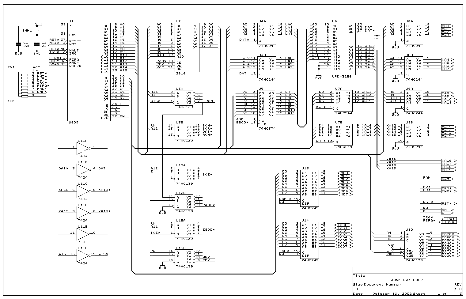
JunkCPU.gif HD6309 CPU section with DAT
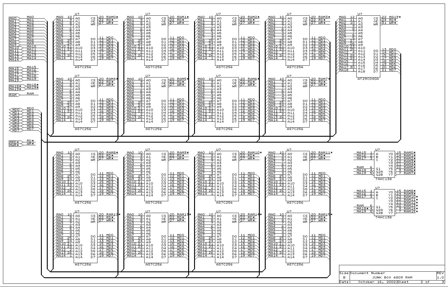
JunkRAM.gif 16 x 32KByte RAM (512K RAM)
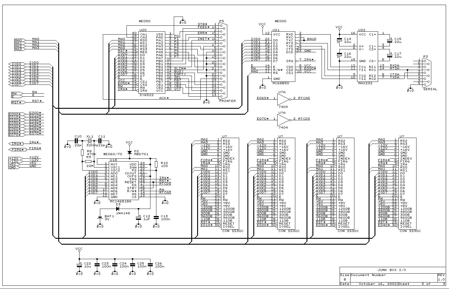
JunkIO.gif Parallel Port, Serial Port, Calendar Clock & SS30 Slots
The Junk Box 6809 system is designed to use old parts that are readily found in my Junk Box.
This includes HD63B09s, 65C22s, MC146818s, 68B50s, 28C16s, 32K x 8 cache SRAM,
29C040s and assorted octal buffers, tranceivers, latches and decoders.
I have enough parts to build two boards. I'm not sure if I'll include the 29C040 or not. I might
save them for the SS30 68HC11F1 project.
The design uses a DAT to map 1 Mbyte of memory on 4K pages. I might use the MSB as a
write protect bit. and only map 512K of SRAM (16 x 32KBytes).
16 October 2002
- The CPU is still missing the reset circuit. I need to include a 74HC14 for reset and NMI.
- R/W and E signals need to be buffered to the SS30 expansion slots.
- Bypass caps need to be added on CPU, RAM & IO.
- Reference designators need to be allocated in order.
- The write strobe to the DAT RAM in the CPU section needs to be gated with E.
- Need to add a power connector (Will use an AT compatible power socket). Note that the SS30C assumes an unregulated input, though chances are that a regulated PC supply will be used. to this end, the regulators on the SS30 boards should be bypassed or removed. I plan to include jumpers on the board for either regulated or unregulated supplies to the SS30C bus.
- I have not included a baud rate clock on the I/O circuit. I need to use a CD4040 with a 4.9152MHz clock and a dip switch to select the baud rate clock to the ACIA.
Memory Map:
68B50 ACIA sits at $E00X
SS30 slot0 sits at $E01X (Floppy Disk Controller)
SS30 slot1 sits at $E02X
SS30 slot2 sits at $E03X
SS30 slot3 sits at $E04X
65C22 VIA sits at $E05X
MC146818 address register sits at $E06X
MC146818 data register sits at $E07X
DAT Bank Select sits at $E800 - $EFFF
ROM (2816) sits at $FXXX (Note that the 2816 is only 2K bytes.)