John's FPGA Page
Page Last Updated 19/10/2007 07:23 PM
Contents:
1. VHDL - References and Tutorials:3. FPGA Prototyping Boards I Use:
3.1 B3-Spartan2+ Board4. FPGA Design Tools:
3.2 Notes on modifying the B3-SRAM module
3.3 B5-X300-Spartan2e Board
3.4 ICST525-01 PLL Clock divider
3.5 Spartan 3 Starter Board
3.6 Spartan 3E Starter Board
3.7 XESS XSA-3S1000
3.8 Memec Design / Avnet V4FX12LC4.1 Xilinx Web Pack ISE:5. FPGA Projects for the B3 & B5-X300:
4.2 Altera Quartus:5.1 System16 - My Initial VHDL CPU Project6. Altera Wishbone Compliant System6801 - By Michael Hasenfratz
5.2 Memio.zip Memory I/O Tool
5.3 Micro8 - A very simple microprocessor
5.4 Micro8a - Adding a Stack
5.5 Micro16 - Very Basic 16 bit machine
5.6 Micro16 - Processing Array
5.7 Motorola 8 bit CPUs
5.8 System01 - 6801 - Working (Incomplete I/O)
5.9 System68 - 6800 - Working
5.10 System05 - 6805 - Work in Progress
5.11 System11 - 68HC11 - Partly Working
5.12 System09 - 6809 SOC - Runs KBug9 with VDU7. Spartan 3 Start Board Project:
8. VHDL & Verilog IP Resource Links:
1. VHDL - References and Tutorials:
The two most common languages used for FPGA design are VHDL and Verilog. I have chosen to use VHDL for my designs for no other reason than the reference books appeared to be a bit cheaper and more readily available. VHDL stands for Very high speed integrated circuit Hardware Description Language
Here are some of the VHDL online Tutorials thrown up by Google:VHDL-online - by Prof. Dr.-Ing. Wolfram H. Glauert, Universität Erlangen-Nürnberg
VHDL Introductory Tutorial - Green Mountain Computing Systems Inc.
Tutorial: Learn by Example - by Weijun Zhang, University of California Riversdale
VHDL Tutorial - Jan Van der Spiegel, University of Pennsylvania
VHDL Cookbook (pdf) - by Peter J. Ashenden - Dept. Computer Science, University of Adelaide South Australia.
A VHDL Tutorial - by Syed Yawar Ali Shah, Concordia University, Montreal.
VHDL Handbook - HARDI Electronics
Heaps of books can be found on Amazon, by using the key words "VHDL", "FPGA" and "XILINX".
2. FPGA Board Vendors:
Here is a list of vendors of low price Xilinx (mostly Spartan) FPGA boards suitable for hobby use:
Burch Electronic Design (Australia)
B5-X300 XC2S300e,
plus a wide range of plug in peripherals.
Digilent Inc (US)
Pegasus Startan2 - XC2S50,
Spartan3 Starter Board - XC3S200, XC3S400, XC3S1000
D2SB - XC2S200e,
D2FT - XC2S300e,
D2XL - XC2S30
Plus a range of CPLD and plugin boards
Xess (US)
XSA50 - XC2S50
XSA100 - XC2S100
XSA200 - XC2S200
XSA1000 - XC3S1000
XSB300E - XC2S300e
XST2 Carrier board
Trenz Electronics (Germany)
TE-XC3S - Spartan3 MicroModules - XC3S200, XC3S400, XC3S1000
TE-??? - Altera Cyclone MicroModule - EP1C12Q240
TE-XC2SE - CPU Development - XC2S300e, XC2S300e
TE-XC2S - Starter Kit - XC2S50, XC2S200
Express IP (UK)
XIP_DEVY - Prototyping FPGA Board - XC2S200
Lots of free IP for their boards
NuHorizons Electronics (US)
Spartan3 Development Board - XC3S400
Spartan3 1500/2000 development board - XC3S1500, XC3S2000
Virtex II FPGA boards are also available.
Also distibutors for Digilent.
Memec Design (US)
A wide range of Spartan 2, Spartan 3, Virtex 2, Virtex 2 Pro and Virtex 4 boards
Too many to list. More intended for professional use.
http://www.fpga-faq.com/
http://www.fpga-faq.com/FPGA_Boards.shtml
The FPGA Frequently Asked Questions Web site has a more comprehensive list of FPGA Prototye Boards.
3. FPGA Prototyping Boards I Use:
3.1 B3-Spartan2+ Board
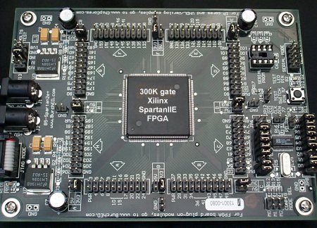
My projects were initially based on the B3-Spartan2+ FPGA board from Burch Electronic Designs .The B3 board uses the 200K gate Xilinx XC2S200. I also used the B3-SRAM 128K x 16bit SRAM module as well as the B3-CPU-IO Interface board for serial comms, keyboard, mouse and VGA video.3.2 Notes on modifying the B3-SRAM module
On the original B3-SRAM module there was no separate output enable (OE*) and write (WR*) signals for upper and lower byte control. To perform byte writes, its was matter of reading the full 16 bits and modifying either the upper or lower byte and writing it back. This meant you had to have more complicated clock generators in 8 bit designs. Tony Burch has remedied this situation on the B5-SRAM module. He has permanently grounded Output Enable (OE*) and has a single Chip Select (CS*) and separate upper and lower byte write enables (WEU*, WEL*) which essentially become read/write lines.
I have modified my B3-SRAM module by cutting the WE* track to U1 on the top of the board and the OE* to J2 pin 19 on the bottom of the board. I have wired U1 pin 12 to J2 pin 19 which becomes WEL* (J2 pin 18 becomes WEU*) and I have grounded the OE* signal on pin 28 of U1 & U2. The Pin outs in the ".ucf" file are for my modified B3-SRAM module and you will have to change them to suit the B5_SRAM. Note that Tony has resequenced the address and Chip select lines on the B5_SRAM.
Some of my designs use the original B3-SRAM module configuration, and some the revised configuration. You will have to check the code to determine which is which.3.3 B5-X300-Spartan2e Board
Burch Electronic Design have superseded the B3 range of boards with the B5 range based around the 300K gate XC2S300E. My projects should work equally well on that board, although the chip pin outs defined in the User Constraint File will probably need to be changed.
3.4 ICST525-01 PLL Clock divider
The B3-Spartan2+ and B5-X300 boards use the ICST525 programmable PLL clock chip for the master clock input with 20 MHz reference clock. There is one of these chips on the main FPGA board, and one on the I/O board. In some of the projects I have used clocks which are multiples of 4.915254 MHz as it is an exact binary multiple of 9600 Baud used by the MiniUart. More recent projects have been designed for a 50MHz clock as this appears to me commonly used on FPGA boards these days. The baud rate clock is derived from a VHDL prescaler on the 50 MHz clock.http://www.icst.com/products/ics525inputForm.html Frequency calculator web page
The following two pages have been pre-calculated:4.915254 MHz ICST525-01 for Memio and System68 at 9600 Baud
9.830508 MHz ICST525-01 for System68 at 19K2 Baud.
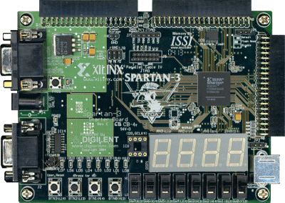
3.5 Spartan 3 Starter Board
The Xilinx Spartan 3 starter board, made by Digilent Inc uses a XC3S200 200K gate device. It has 1MByte of SRAM arranged as 256K x 32 bits. It features VGA connector, RS232 connector, PS/2 Keyboard Connector, Push Buttons, Switches, individual LEDs as well as 4 x 7 segment LED displays. It has 3 x 40 pin expansion connectors for adding on peripheral boards from Digilent. It also has serial flash for storing your FPGA configuration.
The only real draw back with this board is that there is no program flash memory for mass storage, and there are only 3 bits for the VGA output which means only 8 colours.
I have implemented System09 on this board and it only just fits. For US$99 it is not a bad buy. You can get a XC3S1000 version of the board from Digilent for US$149 if you need more logic.
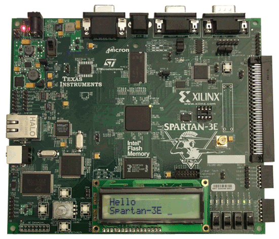
3.6 Spartan 3E Starter Board
The Xilinx Spartan 3E starter board, also made by Digilent Inc uses a XC3S500E FPGA. It has a heap of features, such as Flash Memory, DDR SDRAM, LCD display, ADCs, DACs, RS232, VGA, Ethernet Phy and much more. It has a number of 6 pin headers for adding small 4 bit modules, as well as a Hirose 100 pin FX2 connector, which can be used for such things as the VDEC-1 Video digitizer which I have purchased.
The limitation of the Spartan 3E start board is that there is no SRAM, which means you need a DDR-SDRAM controller core to use it unless you are using EDK. Also, like the Spartan 3 starter board, the VGA connector only has 3 bits connected to it which means there are only 8 colours which limits it's use in displaying digitized images.
This board was given to me as part of a project to validate my 6809 design. Rather than attempting to develop a DDR-SDRAM controller I simply used the internal Block RAM to implement 32KBytes of RAM and an 8KByte Program ROM.
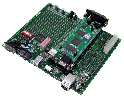
3.7 XESS XSA-3S1000 & XST 3.0
The XSA-3S1000 board from XESS, as the name implies, uses a XC3S1000, 1 million gate Spartan 3 chip. It has a 9 bit (512 colour) VGA output connector as well as a PS/2 keyboard or mouse connector. It has 32MBytes of SDRAM and 4MBits (?) of Flash. The Flash memory is bank selectable and doubles as a FPGA configuration and program code store.
XESS use a CPLD to act as a download controller which connects to the printer port of your computer. They have a rather clever method of downloading FPGA configuration, Flash Program Code, or SDRAM Code. They offer SDRAM controller IP so that your applications can access the SDRAM.
The other good feature of this board is the large number of header pin outs. The board is actually designed to plug into an optional carrier board, but can be used to interface to your own carrier.
The board was purchased so a group of internet friends could develop a PDP-8 project. The large number of uncommitted I/O pins made the board ideal to interface to switch banks and LED display panels as well as other PDP-8 bus devices.
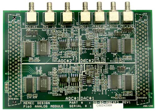
3.8 Memec Design / Avnet V4FX12LC & P160 Analog
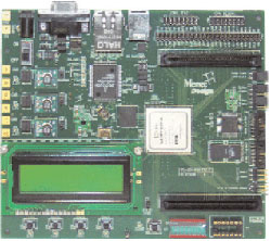
The Memec Design V4FX12LC board uses the Virtex 4 FX12 FPGA which includes a 200MHz Power PC 405 processor in addition to about 500Kgates of programmable logic. This board was purchased for me by work with the idea of doing GPS receiver signal processing. It was bundled with EDK7.1 and BaseX ISE 7.1 as part of the XFest training course offered by Memec in Australia in 2005.
The board features 64MBytes of 16 bit DDR-SDRAM as well as flash memory, push buttons and an LCD display. The V4FX12LC board is really intended for use with EDK. Monta Vista provide a version of Linux for the ML302 (?) board which also runs on the V4FX12LC board. It is only a demo version, so you have to pay $s if you want to do any Linux development with it. Also Monta Vista Linux is designed to run with a soft-core Ethernet controller and does not use either of the two Ethernet controllers built into the V4FX12LC. The Ethernet soft-cores are time limited unless you purchase them I believe.
Memec were taken over by Avnet in 2005/6, but I believe Avnet are still offering the P160 add on modules for this board. The Communications 3 module offers SRAM, VGA and PS/2 interfaces, ADCs and DACs as well as communications interfaces. The ADCs and DACs are only useful for audio frequencies however. There is also high speed data acquisition module for a few hundred dollars which work up into the 10s of Msps range.
You can buy a number of commercial cores such as Floating Point Units for the PPC405 for the Virtex 4 but they cost big bucks and are too expensive for non commercial use. Webpack 8.1 and onwards does include Coregen that includes FPUs, FFTs and so on but I'm not sure however if these cores are designed to interface with the PPC405 on the Virtex 4.
It would be nice to use the V4FX12LC for a software radio:
http://members.optushome.com.au/vk3biz/gnuradio.html
4. FPGA Design Tools
4.1 Xilinx Web Pack ISE:
The Web Pack ISE design software is available free from Xilinx. It is in the order of 100 Megabytes or more so you need a fast cable or ADSL connection if you want to download it via the internet. Alternatively you might want to send off for a CD from Xilinx. Note that Web Pack 5.1i and onwards only works on Windows 2000 and Windows XP. You need to use the older 4.2 version if you are using using Windows 98. As of August 2004 Legacy versions of the Web Pack software where still available on the Xilinx web site.
I've zipped up the working directory produced by Web Pack ISE (Including the User Constraint File) and put them on the web for others to play with. The Xilinx WebPack ISE software is constantly being updated, so some of the project files on this web site may be out of date. WebPack ISE should update the project file, but if it is too old, then you may need to rebuild it for your version.
4.2 Altera Quartus:
Altera's Quartus software is another way to go. I don't have much experience with the Quartus tools although many people swear by them. The book "VHDL" By Douglas Perry which I bought as an introduction to VHDL was based on the Altera software. I did download Quartus once but couldn't work out how to use it. Some people say Quartus is easier to use than the Xilinx software, but I can't say I found that. It probably depends on what you are used to, just like the Intel / Motorola CPU designs of the 70s and 80s.
5. FPGA Projects for the B3 & B5-X300:
5.1 System16 - My Initial VHDL CPU Project
System16 is only a paper design and grew out of my desire to learn VHDL and get a complete processor working on the Burch board. As mentioned, the B3 board did not have individual byte read/write control lines for the upper and lower bytes of RAM, so I decided to make the CPU purely 16 bit and leave upper and lower byte masking to the software [this has changed a little in the evolution of the design]. System16 is a combination of a 6809 design and a mini 68000, in terms of the number of registers, addressing mode terminology and bit operators. I have put a description of System16 up on the web for general interest. I hope to provide a C++ simulator and an assembler and monitor program for it as future projects.
5.2 Memio.zip Memory I/O Tool
Memio is a state sequencer for examining and modifying RAM on the B3-Spartan2+ board. It was developed with the standard WebPackISE 4.2 VHDL tools so you should have no problems getting it to work on that system. It uses a highly hacked version of MiniUart by Ovidiu Lupas from www.opencores.org
Memio assumes you have the B3-FPGA-CPU-IO card connected to connector J3 and the B3-SRAM card connected to J6 and J9. The current clock divider for the UART assumes a 4.915254 MHz clock for 9600bps serial I/O, which gives a nice round division factor for the clock divider.
Commands to Memio are:
M <address> Examine memory location <space bar> <data> Write 16 bit hexadecimal value N Display Next memory location P Display Previous memory location For simplicity only the first 64Kwords of SRAM are used (128Kbytes). Address line A16 is grounded. Data words are 16 bits wide. Command keys and hexadecimal values must be all uppercase (although that could easily be changed). All input characters are echoed back out the UART. This is because I could not get Hyperterm to echo characters locally under windows98 SE.
5.3 Micro8 - A very simple microprocessor
Micro8 started of as a minimal set 4 instruction computer By Tim Boscke designed to fit in a 32 Macrocell CPLD. Only the comments on the top of the listing and the file name remain the same :-) Tim's CPLD CPU does not appear to be on the web any more, but a similar 12 bit CPU can be found at: http://www-student.lut.ac.uk/~elvpc/electronics/fpga/soc.html
I've added to it considerably and run it on the B3-Spartan2+ board. Note that although I have included the add on SRAM in the I/O pin-outs, it does not use the SRAM to print the message, the code should run quite happily without the SRAM module. I put the I/O interface module on connector J3 of the B3 board, but its probably better suited to J8.
Tim's computer had only ADD, NOR , STA and JCC instructions. It had a single carry bit which was set by the JCC (Jump on Carry Clear) instruction. Most microprocessor instructions can be built up using these basic instructions.
In my Micro8 design I have added an 8 bit index register and four addressing modes, Immediate, Absolute, Indexed and PC Relative and I've extended the addressing range from 6 bits or 64 bytes to 11 bits or 2K bytes. The top five bits of the opcode byte determine the operation and addressing mode. the bottom 3 bits of the opcode form the high bits of the address argument. I've also added a Zero (Z) Flag and a Negative (N) flag and corresponding conditional branches that do not change the condition codes.
5.4 Micro8a - Adding a Stack
In my Micro8A I have added a 7 bit stack pointer at $0FF that works down to $080. I've added subroutine calls, Push and Pull registers and interrupts as well as some inherent single byte instructions to operate on the accumulator and index register.5.5 Micro16 - Very Basic 16 bit machine
Micro16 has 8 instructions and two addressing modes: Direct and Indirect. Direct addressing can address 4K Words of Data or Program space while indirect addressing can address 64K Words of data space. The instruction word is 16 bits wide, with 3 bits used for the instruction, 1 bit used for the addressing mode and 12 bits used to form the Direct address. It has an 8 level hardware stack and one interrupt input. It was intended as a substitute for a compact flash state machine. So far I have not managed to get it to work with the Compact Flash, which is a bit unfortunate given how simple it is. I think the problem may have something to do with the speed at which it accesses Compact Flash.5.6 Micro16 - Processing Array
The idea is to implement an array of Micro16 computing elements with shared block RAM memory.
5.7 Motorola 8 bit CPUs
I have coded some of the Motorola CPUs, namely the MC6800 and MC6801, MC6805, MC6809 and MC68HC11. These are works in progress and I have kept a record of their development on their respective web pages.
I originally started off trying to use a VHDL design by Flint Weller for the 6809 as a starting point to learn VHDL. It was a bit too ambitious for someone starting out and I'd recommend something simpler like the Micro8 for newbies. You can find Flint's VHDL core on the Flex User Group page under "File Exchange" however it needs a lot of work.
It was the ambition of one of the Flex User Group members to design an FPGA based Flex system. A description of the 6809 FPGA project can be found under the "Hardware Projects" tab on the Flex Users Groups web site. FLEX is an old disk operating system from the days when computers only had 64KB rather than 640MB. I took up the challenge and started off designing the Micro8, System05 (which I still have not completed), System68 (6800)and eventually the 6809 SOC which I called System09. A number of people have succefully implemented System09 on their FPGA boards.
There is a concerted effort at the moment to collect all the old SWTPC documentation and FLEX Software for prosperity, so if you have any old Flex software, I'm sure they would be happy to hear about it.
5.8 System01 - 6801 - Working (Incomplete I/O)
5.9 System68 - 6800 - Working
5.10 System05 - 6805 - Work in Progress
5.11 System11 - 68HC11 - Partly Working
5.12 System09 - 6809 SOC - Runs KBUG9 with VDU drivers.
6. Altera Wishbone Compliant System6801 - By Michael Hasenfratz
http://www.opencores.org/projects/system6801/
Michael has taken my System68 core and has made it wishbone compliant. He is also looking to add the 6801 peripherals at location $0000 to $001F. The project is being hosted on the OpenCoresweb site. I believe he has ported it to an Altera Device.
Michael Hasenfratz also has a number of Relocating Macro Assemblers for the 68xx family. They are located at ftp://ftp.tothe.net/pubs/shareware/
7. Spartan 3 Starter Board Project:
Spartan3 XC3S200 - System09 with VDU
8. VHDL & Verilog IP Resource Links:
http://www.opencores.org/ Open Cores Repository.
The Open Cores web site seems to be the central repository for a wide variety of computer peripheral designs and is definitely worth checking out. The Open Cores site has a link page to other resources, so I won't include them all here.
http://www.fpgacpu.org Jan Gray's Risc CPU Web Site
Jan Gray has a XR16 RISC CPU , GR000 RISC CPU and XSOC (System on a Chip). He also runs the FPGA CPU mailing list.
http://www.itee.uq.edu.au/~jwilliams/mblaze-uclinux/ John Williams MicroBlaze uCLinux Web Site.
John Williams is a Professor at the School of Information Technology and Electrical Engineering at the University of Queensland. He runs quite an active mailing list for implementing uCLinux on the Xilinx MicroBlaze soft-core processor.
http://www.birdcomputer.ca/ Robert Finch's Bird Computer - FPGA Cores
Robert has a variety of CPU, video, audio, timekeeping and keyboard projects for download on his web site.
Various FPGA projects for the hobbyist. Includes information for connecting devices such as LCD Displays and R/C Servos to FPGAs.
http://www.retromicro.com Doug Hodson's Web Page
Doug has implemented a few projects using the XESS XSA100 FPGA Board. Doug's project page has some examples of VGA video generators. The XSA is quite a nice little board with Flash memory and Dynamic RAM, although the XSA100 uses a smaller FPGA and access to static RAM conflicts with some of the I/O pins. The XSA100 uses a XC2S100 FPGA and can be purchased with the XStend prototyping motherboard. For more details check out http://www.xess.com . They have all the manuals on their web site. The XESS documentation is quite good.
MikeJ's complete PACMAN, Space Invaders, and Galaxians in FPGA !
http://members.iinet.net.au/~msmcdoug/ Mark's Perpetually WIP Home page
Mark's Vic20, ZX81 and Arcade game web page. (Also includes some work on the CoCo).
http://www.geocities.com/gary_l_becker/ Gary's OSI-APPLE-SOC
OSI-SOC is a project to build an enhanced Ohio Scientific Inc Superboard / C1P System On a Chip using a Xilinx FPGA (XC3S1000 Spartan 3 Starter Board). OSI-APPLE-SOC adds an Apple ][e on the same FPGA.
http://www.geocities.com/gary_L_becker/coco3fpga.html CoCo3 FPGA
Gary's CoCo3 on an FPGA.
http://www.madscientistroom.org/fpga/
Randy Thelen has a good User Constraint File generator amongst his FPGA bits and pieces.
http://www.cs.ucr.edu/~dalton/i8051/
The Dalton Project at the University of California Computer Science Dept in Riversdale have an Intel 8051 core. There is a synopsis model as well as C++ simulator for the 8051.
http://www.dte.eis.uva.es/OpenProjects/OpenDSP/index.htm
The Department of Electronic Technology at the University of Valladolid in Spain have an Open DSP design which can be found on their web site.
http://tech-www.informatik.uni-hamburg.de/vhdl/vhdl.html
University of Hamburg VHDL Page. Assorted VHDL tools and microprocessor cores.
http://www.opencores.org/people.cgi/info/jesus
Daniel Wallner's Soft Cores Web site is now on Open Cores with five synthesizable microprocessor cores: PPX16 (PIC16C55, PIC16F84), T80 (Z80), T51 (8051), T65 (6502) and AX8 (90S1200, 90S2313).
K Ring Technologies Semiconductor Indi16 16n bit Forth CPU. Designed for Altera Quartus II software.
http://www.gmvhdl.com/downloads.html
Green Mountains Computing Systems have a MC68HC11 VHDL core as well as VHDL tools and simulators. I tried compiling this core under the Xilinx ISE 4.1 Webpack software and it used 200% of the XC2S200 resource, so it is not an efficient design. Later versions of Xilinx ISE Webpack may be more efficient.
http://www.mcmanis.com/chuck/robotics/fpga/index.html
Chuck McManis has put up a web site with a list of his projects for the B3-SPARTAN2+ board.
http://zxgate.sourceforge.net/
For some fun, projects on the net, using Z80 cpus implemented completely in the FPGA. Daniel Wallner's computers using FPGA T80 cores .
http://server.opensourcedepot.com/
Pat's Open Source Depot. Although there are no FPGA projects listed, Pat used to run a small mailing list for Hobby Computer designers. The mailing list included a small group of people interested in designing with the 6809 and the Burch ED Spartan FPGA boards.
Home