Design and Implementation of a 4-bit ALU
The purpose of this lab is:
- 1. To design a 4-bit ALU
- 2. To implement the ALU on a FPGA or CPLD
- 3. To experimentally check the operation of the ALU
An Arithmetic and Logic Unit (ALU) is a combinational circuit that performs
logic and arithmetic micro-operations on a pair of n-bit operands (ex.
A[3:0] and B[3:0]). The operations performed by an ALU are controlled by
a set of function-select inputs. In this lab you will design a 4-bit
ALU with 3 function-select inputs: Mode M, Select S1 and S0 inputs. The
mode input M selects between a Logic (M=0) and Arithmetic (M=1) operation.
The functions performed by the ALU are specified in Table I.
|
|
||||
|
M = 0 Logic
|
||||
|
|
|
|
FUNCTION
|
OPERATION (bit wise)
|
|
|
|
|
AiBi
|
AND
|
|
|
|
|
Ai + Bi
|
OR
|
|
|
|
|
AiÅ
Bi
|
XOR
|
|
|
|
|
(AiÅ
Bi)
|
XNOR
|
|
M = 1 Arithmetic
|
||||
|
|
|
|
FUNCTION
|
OPERATION
|
|
|
|
|
A
|
Transfer A
|
|
|
|
|
A + 1
|
Increment A by 1
|
|
|
|
|
A + B
|
Add A and B
|
|
|
|
|
A + B + 1
|
Increment the sum of A and B by 1
|
|
|
|
|
A + B'
|
A plus one's complement of B
|
|
|
|
|
A - B
|
Subtract B from A (i.e. B' + A + 1)
|
|
|
|
|
A' + B
|
B plus one's complement of A
|
|
|
|
|
B - A
|
B minus A (or A' + B + 1)
|

Figure 1: Block diagram of the 4-bit ALU.
When doing arithmetic, you need to decide how to represent negative
numbers. As is commonly done in digital systems, negative numbers are represented
in twos complement. This has a number of advantages over the sign
and magnitude representation such as easy addition or subtraction of mixed
positive and negative numbers. Also, the number zero has a unique representation
in twos complement. The twos complement of a n-bit number N is
defined as,
2n - N = (2n - 1 - N) + 1
5 0 1 0 1 --> 1 0 1 0 (bit wise complement)
+ 1
1 0 1 1 (twos complement)
Numbers represented in twos complement lie within the range -(2n-1)
to +(2n-1 - 1). For a 4-bit number this means that
the number is in the range -8 to +7. There is a potential problem
we still need to be aware of when working with two's complement, i.e. over-
and underflow as is illustrated in the example below,
0 1 0 0 (=carry Ci)
+5 0 1 0 1
+4 + 0 1 0 0
+901 0 0 1 = -7!
also,
1 0 0 0 (=carry Ci)
-7 1 0 0 1
-2 + 1 1 1 0
-910 1 1 1 = +7!
Both calculations give the wrong results (-7 instead of +9 or +7
instead of -9) which is caused by the fact that the result +9 or -9 is
out of the allowable range for a 4-bit twos complement number. Whenever
the result is larger than +7 or smaller than -8 there is an overflow or
underflow and the result of the addition or subtraction is wrong. Overflow
and underflow can be easily detected when the carry out of the most significant
stage (i.e. C4 ) is different from the carry out of the previous
stage (i.e. C3).
You can assume that the inputs A and B are in twos complement
when they are presented to the input of the ALU.
b. Design strategies
When designing the ALU we will follow the principle "Divide and Conquer" in order to use a modular design that consists of smaller, more manageable blocks, some of which can be re-used. Instead of designing the 4-bit ALU as one circuit we will first design a one-bit ALU, also called a bit-slice. These bit-slices can then be put together to make a 4-bit ALU.
There are different ways to design a bit-slice of the ALU. One method consists of writing the truth table for the one-bit ALU. This table has 6 inputs (M, S1, S0, C0, Ai and Bi) and two outputs Fi and Ci+1. This can be done but may be tedious when it has to be done by hand.
An
alternative way is to split the ALU into two modules, one Logic and one
Arithmetic module. Designing each module separately will be easier than
designing a bit-slice as one unit. A possible block diagram of the ALU
is shown in Figure 2. It consists of three modules: 2:1 MUX, a Logic unit
and an Arithmetic unit.
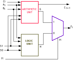
Figure 2: Block diagram of a bit-slice ALU
c.Displaying the results. In order the easily see the output of the ALU you will display the results on the seven-segment displays and the LEDs (LD).
1.The result of the logic operation can be displayed on the LEDs (LD). Use also one of these LEDs to display the overflow flag V.
2.Since you are working with a 4-bit representation for 2's complement numbers, the maximum positive number is +7 and the most negative number is 8. Thus a single seven-segment display can be used to show the magnitude of the number. Use another seven-segment display for the - sign (e.g. use segment g).
3.There is one complication when using more than one of the seven-segment displays on the Digilab board, as can be seens from the connections of the LED segments of the displays. You will notice that the four seven-segment displays share the same cathodes A, B, ..., G). This implies that one cannot directly connect the signals for the segments of the magnitude and sign to these terminals, since that would short the outputs of the gates which would damage the FPGA!. How could you solve this problem? Sketch a possible solution in your lab notebook. (Hint: You can alternate the signals applied to the cathodes between those of the Magnitude and Sign displays. If you do this faster than 30 times per second the eye will not notice the flickering. You will also need to alternate the anode signals). What type of circuit will be needed to accomplish this? You can make use of an on-chip clock, called OSC4 that provides clock signals of 8MHz, 500KHz, 590Hz and 15Hz.
4.Figure
3 shows a schematic of the overall system, consisting of the ALU, Decoder
and Switching circuit, and Displays on the Digilab board.
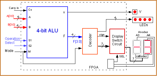
Figure 3: Overall system, including the 4-bit ALU and display units.
d. Tasks: Do the following tasks prior to coming to the lab. Write the answers to all questions in your lab notebook prior to coming to the lab. There is no on-line submission for the pre-lab. Ask the TA to sign pre-lab section in your lab notebook at the start of the lab session. You will also need to include answer to the pre-lab questions in your lab report.
- Design the MUX. You can choose to design the MUX with gates or by writing HDL (VHDL) code. Choose one of the two methods and write the design down in your lab notebook.
- Design of the Logic unit. Here you also have several choices to design this unit:
c.
Write an HDL file
As part of the pre-lab, you can choose any of the three methods. Briefly justify why you chose a particular design method. Explain the design procedure and give the logic diagram or the HDL file. In case you use a MUX, you need also to give the schematic or the HDL file for the MUX.
- Design the arithmetic unit. Again, here you have different choices to design and implement the arithmetic unit. A particularly attractive method is one that makes use of previously designed modules, such as your Full Adder. The arithmetic unit performs basically additions on a set of inputs. By choosing the proper inputs, one can perform a range of operations. This approach is shown in Figure 4. The only blocks that need to be designed are the A Logic and B Logic circuits. You can make use of your previously designed full adder (MYFA).
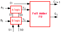
Figure 4: Schematic block diagram of the arithmetic unit.
- Give the truth tables for the Xi and Yi functions with as inputs S1, S0 and Ai, and S1, S0 and Bi, respectively. Fill out the following tables. Notice that in definition table I of the ALU, the variable C0 acts as the Carry input. Depending on the value of C0, one performs the function on the odd or even entries of the definition table I. As an example the first entry is "transfer A" (for C0=0) while the second one is "A+1" (for C0=1); Similarly for A + B and A + B + 1, etc.
|
|
|
|
(A Logic) |
|
|
|
(B Logic) |
|
|
|
|
|
|
|
|
|
|
|
|
|
|
|
|
|
|
|
|
|
|
|
|
|
|
|
|
|
|
|
|
|
|
|
|
|
|
|
|
|
|
|
|
|
|
|
|
|
|
|
|
|
|
|
|
|
|
.
|
|
|
|
|
|
|
|
|
|
|
|
|
|
- Give the K-map for Xi and Yi functions. Find the minimum realization for Xi and Yi.
- Draw the logic diagram for Xi and Yi.
- Design the circuit that detects over- or underflow.
5.Design the switching circuit that is needed to use the two seven-segment displays (see section c3 above).
- 1. PC
- 2. Xilinx Foundation Tools (available on the PCs in the EE Undergraduate Lab)
- 3. Digilab Board
- 4. Protoboard
As this project is more complicated than earlier projects, it will be important that you be very systematic during the design. Each macro should be simulated and errors corrected before you proceed. Failing to do so will make it difficult to debug the system.
Task 1:
- Create a new project in the schematic flow mode: Name it MY4ALU. Place this project in your folder (with your name) on the C:drive.
- Open the schematic editor (the sheet should have the same name as the project: MY4ALU1.sch). This will be your top -level schematic. (Note: Every time you open a new sheet it will be named MY4ALU2.sch, MY4ALU3.sch; all these sheets are part of the top-level schematic. You should use multiple sheets only when your top-level schematic is so large that it does not fit on a single sheet).
- Create macros for each module (carefully read the section on "Creating Macros" in the Xilinx Tutorials - do not use the top sheet as a macro!). This can be done in the Schematic Editor window by selecting TOOLS -> SYMBOL WIZARD.
- Define the underlying source files for the macros.
- Do a functional simulation of the macros (place them on the top level schematic first). Verify the proper operation before proceeding to the next step. This will make debugging much easier. If you find errors in the simulated waveform, debug the circuit. Check your schematic or HDL code. Remember that names of HDL macros should have a maximum of 8 characters. When checking the schematic, use the Probes to add signals (net names) to the simulator Window. This will help you trace the error in a systematic way.
- Make the bit slice (this should be a macro containing several sub macros)
- Make the 4-bit ALU.
- Design and add the circuit that detects overflow V to your schematic.
- Simulate the full 4-bit ALU and verify that all logic and arithmetic operations function properly.
- This task will depend somewhat on the type of board you are planning to use.
- If you are using the Digilab board:
- For the A and B inputs, use the general purpose slide switches SW1-8.
- For the Select and Mode inputs (M, S1, S0 and Cin), you will need to use a short wire that you connect between the corresponding pin of the FPGA and the Vdd or Ground to make the signal 1 or 0, respectively. Use the following colors: Cin: yellow; M: Red; S1: Blue and S0: Black). Check the pins of the Spartan FPGA (XS10XL) to find which pins are available for inputs.
- The result of the logical operations can be displayed on the LEDs (LD). Use also one of these LEDs to indicate when overflow occurs.
- The results of the arithmetic operations are displayed on two seven-segment displays (one for the sign and one for the magnitude). As explained in the pre-lab, this will require the insertion of the switching circuit between the decoder and the displays.
- Can you also display the decimal values of the inputs A and B when used for arithmetic operations?
- If you have a FPGA demoboard:
- Use the 7-segment display U8 to show the result of the arithmetic operation and the LED bar indicator for the logic operations. The sign can be shown on one of the LED segments (e.g. "g") of the second 7-segment display U7. Design the decoders such that in when you select the arithmetic mode (M=1), only the 7-segment LEDs are active and when in the logic mode (M=0), only the LED bar indicator is active. The overflow/underflow bit can be shown on the bar LED. Design and simulate the decoders for the displays. Add them to the schematic.
- For the A and B inputs, use the input switches SW3 on the demoboard.
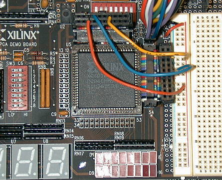
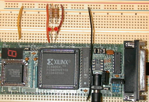
- For the select inputs (Cin, M, S1 and S0) you will need to use a short wire connected to an input of the FPGA and your protoboard. You can connect this wire on the protoboard to ground or 5V depending on the state of the inputs. Check the pin out of the FPGA to find which pins are available for inputs. For a picture of the demoboard with protoboard, click here.
- Make a list of all the inputs and outputs and assign pin numbers to them.
- In case you are using the XS40 board, you have only one 7-segment display available.
- You can use this to display both the arithmetic the logic operations (e.g. segments "b", "c", "e" and "f"), depending on the value of the mode bit, M. For the sign, and the overflow/underflow bit you can use external LEDs connected between one of the available pins of the FPGA (e.g. pins 3, and 4) and the ground (pin 52). This will require that you place the XS40 board on a protoboard. Notice that the current in the diode needs to be limited by placing a resistor of about 330 Ohm in series with the diode. Design and simulate the decoders for the displays. Add them to the schematic.
- The inputs A and B are applied through the parallel port. Remember that for the parallel port D3 and D4, you will need to use the special purpose pads MD0 and MD2, respectively (D3 and D4 are connected to pins 32 and 34 on the XS40 board).
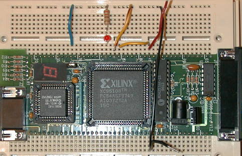
- For the mode bit, M, the select bits, S1 and S0, and the Cin signal you will need to use a short wire connected to the proper input pins of the FPGA and ground or Vdd. The easiest would be to place the XS40 board on a protoboard to make these connections. . Check the pin out of the FPGA to find which pins are available for inputs. Click here for a picture showing some of the connections using a protoboard.
- Make a list of all the inputs and outputs and assign pin numbers to them.
- For the XS95 board there is only one 7-segment display available.
- You can use this to display both the arithmetic, the logic operations (e.g. segments "b", "c", "e" and "f"), depending on the value of the mode bit, M. The decimal point can be used to indicate the sign. To show the overflow/underflow bit, you will need to use an external diode between one of the available pins (e.g. pin 4) of the CPLD and the ground. In order the limit the current in the diode you need to add a resistor of about 330 Ohm in series with the diode. In this case you will need to place the XS95 board on a protoboard to get easy access to the pins. Design and simulate the decoders for the displays. Add them to the schematic.
- The inputs A and B are applied through the parallel port.
- For the mode bit, M, the select bits, S1 and S0, and Cin, you will need to use a short wire connected to the proper input pins of the CPLD and ground or Vdd. The easiest would be to place the XS95 board on a protoboard to make these connections. . Check the pin out of the CPLD to find out which pins are available for inputs. Click here for a picture showing some of the connections using a protoboard.
- Make a list of all the inputs and outputs and assign pin numbers to them.
- Specify the pin location (using the constraint editor or on the schematic), implement and test the ALU.
- It will be instructive to do a timing simulation to get an idea about the overall speed of the circuit.
- Give a demo to the lab instructor and convince him/her that your ALU works properly. The instructor will sign off your lab notebook.
When working on Xilinx, keep the project on the hard disk. At the
end of the lab you should copy your project back to a directory on your
account for future use. If the file is too large, you can easily
zip it by going to the Project Manager winder and selecting FILE-> ARCHIVE
PROJECT. This will zip the entire project with all the necessary project
libraries.
1. Course Title, Lab no, Lab title, your name and date
2. Section on the Pre-lab explaining the design of each block and giving the answers to each task.
3. Section on the lab experiment:
a.
Brief description of the goals.
b. Brief explanation of the design approach, the overall schematic
and of each macro.
c. Copy of the schematics and HDL source code (as a screen capture).
Label the schematics and comment on the source code.
d. Logic simulation (screen capture of the waveforms; label the outputs
to prove that the circuit functions properly).
e. Discussion of the results indicating that the circuit functions
properly.
4.
Conclusion and discussion.
The lab report is an important part of the laboratory. Write it carefully, be clear and well organized. It is the only way to convey that you did a great job in the lab. It is preferred (but not necessary) that you type the lab report.
1. M. Mano and C. Kime, "Logic and Computer Design Fundamentals", 2nd Edition, Prentice Hall, Upper Saddle River, NJ, 2001.2. R. Katz, "Contemporary Logic Design", Benjamin/Cummings Publ., Reading, MA, 1994.3. J. Wakerly, "Digital Design", 3rd Edition, Prentice Hall, Upper Saddle River, 2000.