Planning your FPGA design
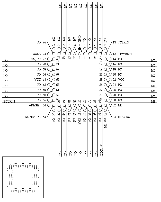
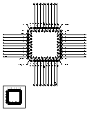 A Xilinx FPGA is physically a square
matrix of CLBs (combinational logic blocks) surrounded by IOBs
(input/output blocks), all interconnected by fusible switch networks.
Most of the pins of the FPGA are tied to the user-programmable IOB
outputs while the rest are used for power, ground, configuration, and
clocking. The XC3000 series pin diagram
shows that as many as 70 pins can be used for input and output by your
design.
A Xilinx FPGA is physically a square
matrix of CLBs (combinational logic blocks) surrounded by IOBs
(input/output blocks), all interconnected by fusible switch networks.
Most of the pins of the FPGA are tied to the user-programmable IOB
outputs while the rest are used for power, ground, configuration, and
clocking. The XC3000 series pin diagram
shows that as many as 70 pins can be used for input and output by your
design.
XC4000 series chips have more power and ground pins and therefore
fewer available I/O pins. Consult The Programmable Logic Data
Book from Xilinx for pin diagrams and explanations. Your choice
of target hardware makes a big impact on which I/O pins you can assign
in your design. See the section discussing GERM,
BORG, or custom FPGA prototyping options.
As with any VHDL design, you should use a well-planned hierarchy of
modules if possible. This allows you to reuse modules in the same or
other projects, and to simulate and debug smaller, simpler functional
units before combining them all.
Clocking
Xilinx FPGAs have special interconnection networks for clock signals,
which are tied to a certain fixed Clock Input pin. Use the
global clock network for the clock input to all your flip
flops. Using a completely synchronous design will simplify simulation
and debugging tremendously. Stay away from asynchronous temptations
such as gated clocks and ripple counters where one flip flop is
clocked by the output of another.
Often a flip-flop with a gated clock can be replaced very easily
by a flip-flop with a clock enable (CE) input. The flip-flops in the
CLBs of Xilinx FPGAs have a CE input which can be inferred from VHDL.
The back of the Xilinx Data Book mentioned above has a
collection of valuable articles about asynchronous design and
related pitfalls.
Synopsys will automatically decide which signals deserve to be placed
on the global clock networks; in fact, sometimes it gets a bit
overzealous and assigns more clock nets than the FPGA has available.
This can be fixed by giving
Design Analyzer a couple of hints before compiling the design.
Created by Scott E. Harrington, Duke Electrical Engineering
 A Xilinx FPGA is physically a square
matrix of CLBs (combinational logic blocks) surrounded by IOBs
(input/output blocks), all interconnected by fusible switch networks.
Most of the pins of the FPGA are tied to the user-programmable IOB
outputs while the rest are used for power, ground, configuration, and
clocking. The XC3000 series pin diagram
shows that as many as 70 pins can be used for input and output by your
design.
A Xilinx FPGA is physically a square
matrix of CLBs (combinational logic blocks) surrounded by IOBs
(input/output blocks), all interconnected by fusible switch networks.
Most of the pins of the FPGA are tied to the user-programmable IOB
outputs while the rest are used for power, ground, configuration, and
clocking. The XC3000 series pin diagram
shows that as many as 70 pins can be used for input and output by your
design.