TABLE OF CONTENTS
1- Introduction ................................................................................................................................ 2
2- Setting up the environment to run the Synopsys VHDL simulation tools .................................. 2
3- VHDL: Basic Language Organization ....................................................................................... 3
4- Examples .................................................................................................................................... 4
4.1- Full Adder ............................................................................................................................ 4
4.1.1- Structural Description ................................................................................................ 4
4.1.2- Behavioral Descriptions ........................................................................................... 15
4.1.3- Stimulator ................................................................................................................. 17
4.1.4- Test Bench for Full Adder ........................................................................................ 19
4.2- Register .............................................................................................................................. 21
4.2.1- Structural Description .............................................................................................. 21
4.2.2- Mixed Description .................................................................................................... 27
4.2.3- Behavioral Description ............................................................................................. 29
4.3- Counter ............................................................................................................................. 31
4.3.1- BCD Counter ............................................................................................................ 31
4.3.2- 3 Digit Counter ......................................................................................................... 38
4.4- Multiplier ........................................................................................................................... 43
4.4.1- Unsigned 4x4 Bit Multiplier .................................................................................... 43
4.4.2- Unsigned 8x8 Bit Multiplier .................................................................................... 44
4.4.3- Signed 8x8 Bit Multiplier ......................................................................................... 45
4- EXAMPLES
4.1- FULL ADDER
VHDL code for full adder is generated using three different modeling styles i.e Structural, Data-flow and Algorithmic. Thus three different architectures are written for the same design entity FULL_ADDER.
4.1.1- Structural Description:
In Structural description, Structural architecture of the design entity describes it in terms of interconnected components. Each component may be in turn described as interconnected subcomponents or behavioral in terms of built-in functions.
The first step in writing VHDL code for structural architectures is to write the codes for components in separate design entities and analyze them. Analysis creates simulation files in WORK directory. Using those files in the configuration commands of the design code of parent circuit, allows us to use those design entities as components in our parent circuit.
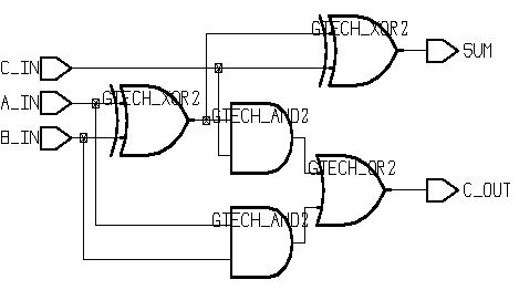
Fig 1: Full Adder Circuit
In the generation of the structural code for Full adder, we will generate VHDL code of all three components i.e XOR, AND and OR gates as shown in the figure 1, in the separate design entities.
4.1.1.1- XOR gate:
Using any text editor (xedit, emacs, etc.), write the VHDL code of XOR gate as given below and save it in file XOR2.vhd
entity XOR_2 is
port (
A, B : in BIT;
Z : out BIT);
end XOR_2;
architecture DATA_FLOW of XOR_2 is
begin
Z <= A xor B;
end DATA_FLOW;
architecture ALGORITHM of XOR_2 is
begin
process(A, B)
begin
if A = B then
Z <= '0';
else
Z <= '1';
end if;
end process;
end ALGORITHM;
Two different architectures ALGORITHM & DATA_FLOW, of the same design entity XOR_2 are given.
4.1.1.2- Analysis:
Analysis is done to check the design for errors and to create simulation files, that will be saved in the WORK directory. Analysis may be performed by using gvan (Graphical VHDL ANalyzer). While you are in your VHDL directory, at UNIX prompt type:
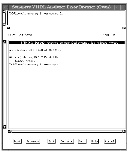
Synopsys VHDL Analyzer Error Browser (Gvan) window will appear as shown in figure 2. Any error contained in the source code will be displayed in the central part of the window. Errors can be corrected by opening your original file (XOR2.vhd) by using any text editor. After correcting the errors, re-analyze the file by using above command. If no error reported, exit the window by clicking Cancel button in the Synopsys VHDL Analyzer Error Browser (Gvan) window.
Fig 2: Synopsys VHDL Analyzer Error Browser (Gvan)
4.1.1.3- Simulation:
Simulation is done to check the dynamic behavior of the design entity. Simulation is done by vhdldbx command. While you are in your VHDL directory, at UNIX prompt type:
Vhdldbx - Select Simulator Arguments window will appear, as shown in figure 3.
Fig 3: Vhdldbx - Select Simulator Arguments
Check that the selected library is DEFAULT. Select any of the two entity-architecture pairs: XOR_2__ALGORITHM or XOR_2__DATA_FLOW from the Design window. Click OK.
Synopsys VHDL Debugger (Vhdldbx) window will appear as shown in figure 4, with your VHDL source code in the upper half of the window. Click on the line, at the most bottom part of the window, to invoke the Command line prompt (#).
To trace the signals, enter at the Command line:
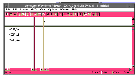
After some time, Synopsys Waveform Viewer window will appear, as shown in figure 5. The next step is to assign values to the inputs. At the Command line in Synopsys VHDL Debugger window, enter
# assign `1' A
# assign `1' B
To run the simulation for 10 ns, enter
Make sure that the number of runs is specified (10 in this case), otherwise your simulation cycle will enter into an infinite loop and you will have to kill that simulation job.
Fig 4: Synopsys VHDL Debugger (Vhdldbx)
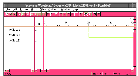
The waveform for selected signals will appear in the Synopsys Waveform Viewer window. To see the complete waveform, select View -> Full Fit from the top menu bar. Give new values and run the simulator for another time period. Figure 6 shows the result of the simulation.
You can print the results by selecting File -> Print. Click on Print to File in the Print Options window and then enter a name for the file with extension .ps, say XOR_SIM.ps. Click OK.
Fig 5: Synopsys Waveform Viewer
Fig 6: Simulation Result of XOR_2
At the UNIX prompt, enter:
Now exit the Synopsys VHDL Debugger (Vhdldbx) window by clicking on Execute -> Quit.
4.1.1.4- Elaboration:
Elaborate command is used to build a design from a VHDL entity and architecture or a VHDL configuration. To elaborate a design, enter the following command from your UNIX prompt:
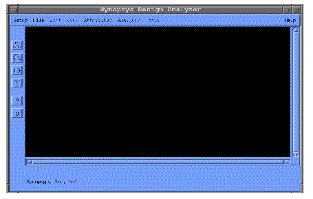
Synopsys Design Analyzer window will open as shown in figure 7.
Fig 7: Synopsys Design Analyzer
Click on File -> Analyze. Analyze File window will appear. Select XOR2.vhd and click OK. Analyze window will appear. After some time if you receive a 1 at the end of analysis, its mean your analysis is successful. If you do not receive a 1, then there are some errors in your VHDL code. Go back and correct them.
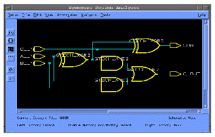
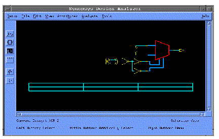
From Synopsys Design Analyzer window, click on File -> Elaborate. Elaborate design window will appear as shown in figure 8. Select library WORK. Two designs will be displayed: XOR_2(ALGORITHM) and XOR_2(DATA_FLOW). Select XOR_2(ALGORITHM) and click OK. You will see entity name (XOR_2) with a box in the center of Synopsys Design Analyzer window. Double click on it. You will see XOR_2 gate with its input/output ports. Double click on it and you will see schematic diagram of XOR gate as shown in figure 9. Follow the same steps for XOR_2(DATA_FLOW). The gate level schematic diagram is shown in Figure 10. It can be seen that the DATA_FLOW architecture is implemented by a built-in XOR gate.
Fig 9: Synopsys Design Analyzer (ALGORITHM design of XOR_2)
Fig 10: Data_Flow Design of XOR_2
4.1.1.5- AND gate:
Generate and save the VHDL code of AND gate, as given below, in file AND2.vhd
entity AND_2 is
port (
A, B : in BIT;
Z : out BIT);
end AND_2;
architecture DATA_FLOW of AND_2 is
begin
Z <= A and B;
end DATA_FLOW;
architecture ALGORITHM of AND_2 is
begin
process(A, B)
begin
if (A = '1' and B = '1') then
Z <= '1';
else
Z <= '0';
end if;
end process;
end ALGORITHM;
Again two different architectures ALGORITHM & DATA_FLOW of the same design entity AND_2 are given.
Analyze and Simulate it as before.
4.1.1.6- OR gate:
Generate and save the VHDL code of OR gate, as given below, in file OR2.vhd.
entity OR_2 is
port (
A, B : in BIT;
Z : out BIT);
end OR_2;
architecture DATA_FLOW of OR_2 is
begin
Z <= A or B;
end DATA_FLOW;
architecture ALGORITHM of OR_2 is
process(A, B)
begin
if (A = '0' and B = '0') then
Z <= '0';
else
Z <= '1';
end if;
end process;
end ALGORITHM;
Analyze and simulate it.
4.1.1.7- Full Adder circuit:
Now you have generated and analyzed all three components of full adder. The last step is to connenect the component together. VHDL code of structural Full Adder is given below. Save it in file FULL_ADDER_STRUC.vhd.
entity FULL_ADDER is
port (
A_IN, B_IN, C_IN : in BIT;
SUM, C_OUT :out BIT);
end FULL_ADDER;
architecture STRUCTURE of FULL_ADDER is
-- Component declarations
component XOR_2
port (
A, B : in BIT;
Z : out BIT);
end component;
component AND_2
port (
A, B : in BIT;
Z : out BIT);
end component;
component OR_2
port (
A, B : in BIT;
Z : out BIT);
end component;
-- Configuration specifications
for all : XOR_2 use entity WORK.XOR_2(ALGORITHM);
for all : AND_2 use entity WORK.AND_2(ALGORITHM);
for O1 : OR_2 use entity WORK.OR_2(ALGORITHM);
-- Signal declarations
signal S1, S2, S3 : BIT;
begin
-- Component Instantiations using named association
X1 : XOR_2 port map (A => A_IN, B => B_IN, Z => S1);
X2 : XOR_2 port map (A => S1, B => C_IN, Z => SUM);
A1 : AND_2 port map (A => S1, B => C_IN, Z => S2);
A2 : AND_2 port map (A => A_IN, B => B_IN, Z => S3);
O1 : OR_2 port map (A => S2, B => S3, Z => C_OUT);
end STRUCTURE;
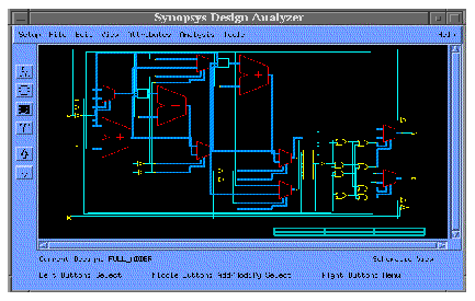
Components are first declared and then connected together by using port map command. Only ALGORITHM architectures of XOR_2, AND_2 and OR_2 entities are used in configuration specifications. You can also select DATA_FLOW architectures by just replacing DATA_FLOW with ALGORITHM in the configuration specification commands. Analyze the code and then elaborate it. You will see the design as shown in figure 11.
Fig 11: Structural Design of Full Adder
4.1.2- Behavioral Descriptions:
Two more VHDL descriptions (Data-flow and Algorithmic) of Full Adder are shown below. Save it in file FULL_ADDER_BEHAV.vhd.
entity FULL_ADDER is
port (
A_IN, B_IN, C_IN : in BIT;
SUM, C_OUT :out BIT);
end FULL_ADDER;
architecture DATA_FLOW of FULL_ADDER is
-- Signal declarations
signal S1, S2, S3 : BIT;
begin
S1 <= A_IN xor B_IN;
SUM <= S1 xor C_IN;
S2 <= S1 and C_IN;
S3 <= A_IN and B_IN;
C_OUT <= S2 or S3;
end DATA_FLOW;
architecture ALGORITHM of FULL_ADDER is
begin
process (A_IN ,B_IN, C_IN)
variable S : BIT_VECTOR(1 to 3);
variable NUM : INTEGER range 0 to 3 := 0;
begin
S := A_IN & B_IN & C_IN;
for I in 1 to 3 loop
if S(I) = '1' then
NUM := NUM + 1;
end if;
end loop;
case NUM is
when 0 => C_OUT <='0'; SUM <= '0';
when 1 => C_OUT <='0'; SUM <= '1';
when 2 => C_OUT <='1'; SUM <= '0';
when 3 => C_OUT <='1'; SUM <= '1';
end case;
end process;
end ALGORITHM ;
Analyze the code and then elaborate both Dataflow and Algorithmic designs. The results are shown in figures 12 and 13.
Fig 12: Dataflow Design of Full Adder
Fig 13: Algorithmic Design of Full Adder
4.1.3- Stimulator:
To generate 3 inputs for full adder, write the code of 3 bit Stimulator as below and save it in file
STIMULATOR.vhd. Port specifications of Stimulator are given in figure 14.
Fig 14: Port Specifications of Stimulator
entity STIMULATOR is
port (
O1, O2, O3 : out BIT);
end STIMULATOR;
architecture ALGORITHM of STIMULATOR is
begin
-- Concurrent processes
STIMULATOR1 : process
begin
O1 <= '0';
wait for 40 ns;
O1 <= '1';
wait for 40 ns;
end process;
STIMULATOR2 : process
begin
O2 <= '0';
wait for 20 ns;
O2 <= '1';
wait for 20 ns;
end process;
STIMULATOR3 : process
begin
O3 <= '0';
wait for 10 ns;
O3 <= '1';
wait for 10 ns;
end process;
end ALGORITHM;
4.1.4- Test Bench for Full Adder:
In the end connect STIMULATOR and FULL_ADDER together (figure 15), by port mapping to get the test bench for the simulation of Full Adder, as given below. Save it in file BENCH_FA.vhd.
Fig 15: Test Bench of Full Adder
entity BENCH_FA is
end BENCH_FA;
architecture STRUCTURE of BENCH_FA is
-- Component declarations
component STIMULATOR
port (
O1, O2, O3 : out BIT);
end component;
component FULL_ADDER
port (
A_IN, B_IN, C_IN : in BIT;
SUM, C_OUT :out BIT);
end component;
-- Configuration specifications
for ST : STIMULATOR use entity WORK.STIMULATOR(ALGORITHM);
for FA : FULL_ADDER use entity WORK.FULL_ADDER(STRUCTURE);
-- Signal declarations
signal S1, S2, S3, SUM_OUT, CARRY_OUT : BIT;
begin
-- Component Instantiations using positional association
ST : STIMULATOR port map (S1, S2, S3);
FA : FULL_ADDER port map (S1, S2, S3, SUM_OUT, CARRY_OUT);
end STRUCTURE;
Structural architecture of Full Adder has been used in this bench. You can use any one of 3 architectures by changing STRUCTURE to DATA_FLOW or ALGORITHM in the configuration specification command of Full Adder.
Analyze the bench and then simulate it. In the Command line of Synopsys VHDL Debugger (Vhdldbx) window, type:
The simulation result is given on figure 16.
4.2- REGISTER
Design entity of Register is described using two architectures i.e. Structural and Behavioral.
4.2.1- Structural Description:
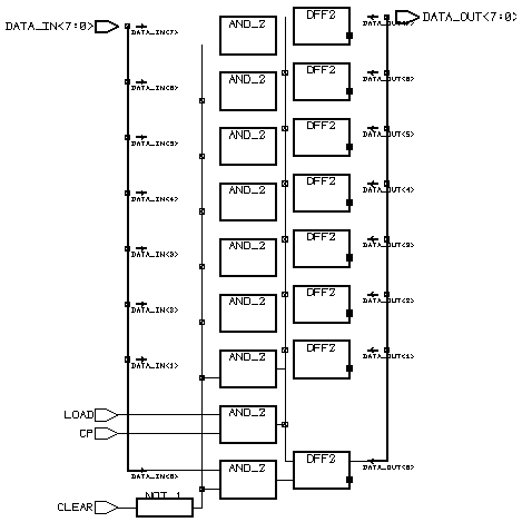
In the generation of the structural code for 8 bit Register, we will generate VHDL code of all three components i.e DFF, AND and NOT gates, as shown in the figure 17, in the separate design entities.
Fig 17: 8 bit Register citcuit
4.2.1.1- D Flip Flop:
Using any text editor, write the VHDL code of DFF as given below and save it in file DFF1.vhd.
entity DFF1 is
port (
D, CP : in BIT;
Q, QNOT : out BIT);
end DFF1;
architecture BEHAVIOUR of DFF1 is
begin
process
variable Q_INSIDE : BIT;
begin
wait until (CP = '1'and CP'event);
-- Wait for the rizing edge of clock
Q_INSIDE := D;
Q <= Q_INSIDE;
QNOT <= not Q_INSIDE;
end process;
end BEHAVIOUR;
Variable is used inside the architecture instead of signal whose value will change instantaneously. The values assigned to signals does not change immediately. `:=' is variable assignment operator. Note that variables are declared inside the process statements.
In CP'event, event is a predefined attribute. It has a value of type BOOLEAN. If an event will occur on CP, CP'event will become TRUE; otherwise it is false.
Another code of DFF is given below. (Save it in file DFF2.vhd).
entity DFF2 is
port (
D, CP : in BIT;
Q, QNOT : buffer BIT);
end DFF2;
architecture BEHAVIOUR of DFF2 is
begin
process(CP)
begin
if (CP = '1'and CP'event)
then Q <= D;
end if;
end process;
QNOT <= not Q;
end BEHAVIOUR;
Note that in the interface part, mode of the ports Q and QNOT is buffer instead of out.
VHDL provides five port modes
in: Information flows only into the design entity.
out: Information flows only out of the design entity.
input: Information flows into and out of the design entity. A value can be read and assigned. The value read is that of the port's incoming value, not the assigned value (if any).
buffer: Information flows into and out of the design entity. It is similar to out, but it can be read. The value read is the assigned value.
linkage: Information flows into and out of the design entity.
In DFF2, the mode of the ports Q and QNOT is buffer, so we don't need an internal variable.
Analyze DFF1.vhd and DFF2.vhd and simulate to see that they have same dynamic behavior. Then elaborate the two entities, you will get the results as shown in figure 18 and 19.
4.2.1.2- AND gate:
AND_2 design entity (already saved in AND2.vhd file) will be used in Structural Register.
4.2.1.3- NOT gate:
Generate and save the VHDL code of inverter, as given below, in file NOT1.vhd
entity NOT_1 is
port (
A : in BIT;
A_BAR : out BIT);
end NOT_1;
architecture DATA_FLOW of NOT_1 is
begin
A_BAR <= not A ;
end DATA_FLOW;
architecture ALGORITHM of NOT_1 is
begin
process(A)
begin
Fig 18: DFF1
Fig 19: DFF2
if A = '1' then
A_BAR <= '0';
else
A_BAR <= '1';
end if;
end process;
end ALGORITHM;
Analyze and simulate it.
4.2.1.4- Register:
Structural description of 8 bit register, using components DFF, AND gate and Inverter, is given below. Save it in file REGISTER8_STRUC.vhd.
entity REGISTER8_1 is
port (
CP, CLEAR, LOAD : in BIT;
DATA_IN : in BIT_VECTOR(7 downto 0);
DATA_OUT : buffer BIT_VECTOR(7 downto 0));
end REGISTER8_1;
use WORK.PACKAGE1.all;
architecture STRUCTURE of REGISTER8_1 is
-- Signal declarations
signal D : BIT_VECTOR(7 downto 0);
signal N_CLEAR, CLK : BIT;
begin
STAGES:
for I in 0 to 7 generate
LOWBIT:
if I = 0 generate
B1: block
for FF1 : DFF2 use entity WORK.DFF2(BEHAVIOUR);
for A1,A2 : AND_2 use entity WORK.AND_2(ALGORITHM);
for N1 : NOT_1 use entity WORK.NOT_1(ALGORITHM);
begin
N1 : NOT_1 port map(CLEAR, N_CLEAR);
A1 : AND_2 port map(DATA_IN(0), N_CLEAR, D(0));
A2 : AND_2 port map(LOAD, CP, CLK);
FF1 : DFF2 port map(CLK, D(0), DATA_OUT(0), open);
end block;
end generate;
OTHERBITS:
if I /= 0 generate
B2: block
for FF2 : DFF2 use entity WORK.DFF2(BEHAVIOUR);
for A3 : AND_2 use entity WORK.AND_2(ALGORITHM);
begin
A3 : AND_2 port map(DATA_IN(I), N_CLEAR, D(I));
FF2 : DFF2 port map (CLK, D(I), DATA_OUT(I), open);
end block;
end generate;
end generate;
end STRUCTURE;
Instead of declaring components in architecture, they are declared in package, PACKAGE1 as shown below. Save it in file PACKAGE1.vhd.
package PACKAGE1 is
-- Component declarations
component DFF2
port (
CP, D : in BIT;
Q, QNOT : buffer BIT);
end component;
component AND_2
port (
A, B : in BIT;
Z : out BIT);
end component;
component NOT_1
port (
A : in BIT;
A_BAR : out BIT);
end component;
end PACKAGE1;
VHDL structural descriptions of logic schematics often use the same set of components and rewriting component declarations for every logic schematic can be tedious; this problem can addressed by packages. Package declaration can contain component declarations, signal declarations, type & subtype declarations, function declarations, procedure declarations, etc.
First analyze PACKAGE1.vhd and then analyze REGISTER8_STRUC.vhd. Simulate the Structural description of Register and then Elaborate it. You will get logic schematic as shown in figure 20.
Fig 20: Structural Design of 8 bit Register
4.2.2- Mixed Description:
We can mix different implementation styles together. In the following example an 8 bit Register has been implemented using a mixed description, containing both structural and dataflow implementation styles. Save it in file REGISTER8_MIXED.vhd.
entity REGISTER8_1 is
port (
CP, CLEAR, LOAD : in BIT;
DATA_IN : in BIT_VECTOR(7 downto 0);
DATA_OUT : buffer BIT_VECTOR(7 downto 0));
end REGISTER8_1;
architecture MIXED_IMPLEMENTATION of REGISTER8_1 is
-- Component declarations
component DFF2
port (
CP, D : in BIT;
Q, QNOT : buffer BIT);
end component;
-- Signal declarations
signal D : BIT_VECTOR(7 downto 0);
signal N_CLEAR, CLK : BIT;
begin
STAGES:
for I in 0 to 7 generate
LOWBIT:
if I = 0 generate
B1: block
for FF1 : DFF2 use entity WORK.DFF2(BEHAVIOUR);
begin
N_CLEAR <= not CLEAR;
D(0) <= DATA_IN(0) and N_CLEAR;
CLK <= LOAD and CP;
FF1 : DFF2 port map(CLK, D(0), DATA_OUT(0), open);
end block;
end generate;
OTHERBITS:
if I /= 0 generate
B2: block
for FF2 : DFF2 use entity WORK.DFF2(BEHAVIOUR);
begin
D(I) <= DATA_IN(I) and N_CLEAR;
FF2 : DFF2 port map (CLK, D(I), DATA_OUT(I), open);
end block;
end generate;
end generate;
end MIXED_IMPLEMENTATION;
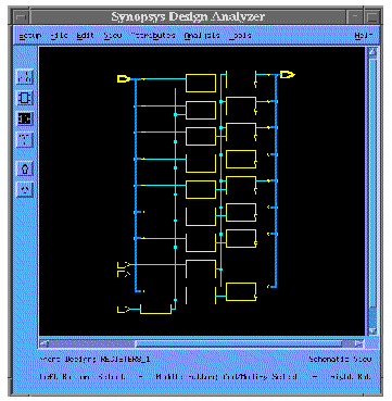
Analyze the file, simulate it to check the dynamic behavior and then elaborate it, you will see the logic schematic as shown in figure 21.
Fig 21: Mixed Implementation of 8 bit Register
4.2.3- Behavioral Description:
Behavioral description of Register is described below. Save it in file REGISTER8_BEHAV.vhd.
package PACK is
type VECTOR8 is array (7 downto 0) of BIT;
end PACK;
use WORK.PACK.all;
entity REGISTER8_2 is
port (
CP, CLEAR, LOAD : in BIT;
DATA_IN : in VECTOR8;
DATA_OUT : buffer VECTOR8);
end REGISTER8_2;
architecture BEHAVIOUR of REGISTER8_2 is
begin
process(CP)
begin
if (CP = '1'and CP'event) then
if CLEAR ='1'then
DATA_OUT <= VECTOR8'(others => '0');
elsif LOAD = '1' then
DATA_OUT <= DATA_IN;
end if;
end if;
end process;
end BEHAVIOUR;
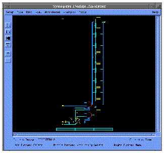
A user defined Type VECTOR8 is declared inside package PACK which is also saved in the same file. others command is used to make all the bits of VECTOR8 zeroes. Analyze the file, simulate it to check the dynamic behavior and then elaborate it, you will see the logic schematic as shown in figure 22.
Fig 22: Behavioral Design of 8 bit Register
4.3- COUNTER
In this part two descriptions of BCD Counter are given and then BCD Counter is upgraded to 3 digit Counter. Test benches for both counters are also given.
4.3.1- BCD Counter:
Algorithmic description of BCD counter is given below. Save it in file BCD_COUNTER1.vhd.
library IEEE ;
use IEEE.STD_LOGIC_1164.all;
entity COUNTER is
port (
CP, RESET : in STD_LOGIC ;
COUNT : buffer STD_LOGIC_VECTOR(3 downto 0));
end COUNTER;
architecture ALGORITHM1 of COUNTER is
type STATE_TYPE is range 0 to 9;
signal CURRENT_STATE : STATE_TYPE;
begin
COMBINATIONAL : process(CURRENT_STATE)
begin
case CURRENT_STATE is
when 0 => COUNT <= "0000";
when 1 => COUNT <= "0001";
when 2 => COUNT <= "0010";
when 3 => COUNT <= "0011";
when 4 => COUNT <= "0100";
when 5 => COUNT <= "0101";
when 6 => COUNT <= "0110";
when 7 => COUNT <= "0111";
when 8 => COUNT <= "1000";
when 9 => COUNT <= "1001";
end case ;
end process;
SEQUENTIAL: process
begin
wait until (CP = '1') and CP'event;
if (RESET = '0') and (CURRENT_STATE /= 9) then
CURRENT_STATE <= CURRENT_STATE + 1;
else
CURRENT_STATE <= 0;
end if;
end process;
end ALGORITHM1;
In earlier examples, we were using type of information as BIT or BIT_VECTOR. The declaration of predefined type BIT and BIT_VECTOR is provided in the package STANDARD, which is linked to our VHDL files by default. In the above VHDL code, the type of information is STD_LOGIC, which is used to represent values in standard 9-valued logic systems. It is declared in package STD_LOGIC_1164 as
type STD_LOGIC is (`U','X','0','1','Z','W','L','H','-');
This package is located in library IEEE. We can use this package by first using the library command and then using use command.
The architecture ALGORITHUM1, contains two concurrent processes, COMBINATIONAL and SEQUENTIAL. A user defined type STATE_TYPE is declared inside architecture. case statement is used to select the value of COUNT depending on the value of CURRENT_STATE.
Analyze the design and then Elaborate it. You will get a design as shown in figure 23.
Another Algorithmic description of BCD Counter is given below. Save it in file BCD_COUNTER2.vhd.
library IEEE;
use IEEE.STD_LOGIC_1164.all;
use IEEE.STD_LOGIC_UNSIGNED.all;
entity COUNTER is
port (
CP, RESET : in STD_LOGIC;
COUNT : buffer STD_LOGIC_VECTOR(3 downto 0));
end COUNTER;
architecture ALGORITHM2 of COUNTER is
constant ZERO : STD_LOGIC_VECTOR(3 downto 0) := "0000";
constant NINE : STD_LOGIC_VECTOR(3 downto 0) := "1001";
begin
process(CP, RESET)
begin
if RESET = '1' then
Fig 23: BCD Counter(Algorithum1)
COUNT <= ZERO;
elsif ((CP = '1') AND CP'event) then
if COUNT = NINE then
COUNT <= ZERO;
else
COUNT <= COUNT + '1';
end if;
end if;
end process;
end ALGORITHM2;
The use of `+' is an example of Operator Overloading, which is described in STD_LOGIC_UNSIGNED package of IEEE library.
Analyze the design and then Elaborate it. You will get a design as shown in figure 24.
Fig 24: BCD Counter (Algorithum2)
4.3.1.1- Clock:
To generate the test bench for the simulation of BCD Counter, we need a clock, whose VHDL code is given below. Save it in file CLOCK.vhd. Port specifications for Clock are shown in figure
25.
Fig 25: Port Specifications of Clock
library IEEE;
use IEEE.STD_LOGIC_1164.all;
entity CLOCK is
generic (
HALF_PERIOD : time := 5 ns);
port (
CP : out STD_LOGIC);
end CLOCK;
architecture BEHAVIOR of CLOCK is
begin
process
begin
CP <= '1';
wait for HALF_PERIOD;
CP <= '0';
wait for HALF_PERIOD;
end process;
end BEHAVIOR;
generic is used in the interface part of entity CLOCK. Using generics allows us to pass values to the entity when that entity is instantiated.
Analyze and simulate the above code.
4.3.1.2- Test Bench for BCD Counter:
In order to do the simulation of BCD Counter, a test bench has been generated by connecting CLOCK and COUNTER together (figure 26), as given below. Save it in file BENCH_COUNTER.vhd.
Fig 26: Test bench of BCD Counter
library IEEE;
use IEEE.STD_LOGIC_1164.all;
entity BENCH_COUNTER is
generic (
HALF_PERIOD : time := 5 ns);
end BENCH_COUNTER;
architecture STRUCTURE of BENCH_COUNTER is
-- Component declarations
component CLOCK
generic (
HALF_PERIOD : time := 5 ns);
port (
CP : out STD_LOGIC);
end component;
component COUNTER
port (
CP, RESET : in STD_LOGIC;
COUNT : buffer STD_LOGIC_VECTOR(3 downto 0));
end component;
-- Configuration specifications
for CLK1 : CLOCK use entity WORK.CLOCK(BEHAVIOR);
for CUNTR : COUNTER use entity WORK.COUNTER(ALGORITHM2);
-- Signal declarations
signal CP, RESET : STD_LOGIC;
signal COUNT : STD_LOGIC_VECTOR(3 downto 0);
signal STOP : BOOLEAN;
begin
-- Component Instantiations using positional association
CLK1 : CLOCK generic map(HALF_PERIOD)
port map(CP);
CUNTR : COUNTER port map(CP, RESET, COUNT);
RESETTING : process
begin
wait on CP;
RESET <= '0';
for I in 1 to 2 loop
for I in 1 to 2 loop
wait for HALF_PERIOD;
end loop;
RESET <= not RESET;
end loop;
-- To stop the process
wait until STOP'event;
end process;
end STRUCTURE;
ALGORITHM2 of COUNTER entity is used. You can use ALGORITHM1 by simply replacing ALGORITHM1 with ALGORITHM2 in the configuration specification command of COUNTER.
A concurrent process RESETTING is given for the asynchronous resetting.
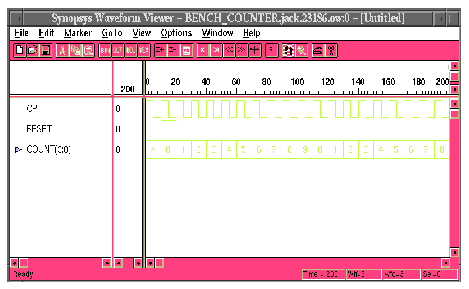
Analyze the bench and then simulate it. In the Command line of Synopsys VHDL Debugger (Vhdldbx) window, type:
# trace CP RESET COUNT
# run 200
You will get simulation result as shown in figure 27.
Fig 27: Simulation result of test bench of BCD Counter
4.3.2- 3 Digit Counter:
ALGORITHM2 architecture of BCD Counter has been upgraded to construct a 3 digit Counter that will permit counting from 0 to 999. Save it in file BCD_COUNTER_3DIGIT.vhd.
library IEEE;
use IEEE.STD_LOGIC_1164.all;
use IEEE.STD_LOGIC_UNSIGNED.all;
entity COUNTER_3DIGIT is
port (
CP, RESET : in STD_LOGIC;
COUNT : buffer STD_LOGIC_VECTOR(11 downto 0));
end COUNTER_3DIGIT;
architecture ALGORITHM of COUNTER_3DIGIT is
signal MSD, LSD2, LSD : STD_LOGIC_VECTOR(3 downto 0);
constant ZERO : STD_LOGIC_VECTOR(3 downto 0) := "0000";
constant NINE : STD_LOGIC_VECTOR(3 downto 0) := "1001";
begin
process(CP, RESET)
begin
if RESET = '1' then
LSD <= ZERO;
LSD2 <= ZERO;
MSD <= ZERO;
elsif ((CP = '1') AND CP'event) then
if LSD = NINE then
LSD <= ZERO;
if LSD2 = NINE then
LSD2 <= ZERO;
if MSD = NINE then
MSD <= ZERO;
else
MSD <= MSD + '1';
end if;
else
LSD2 <= LSD2 + '1';
end if;
else
LSD <= LSD + '1';
end if;
end if;
end process;
COUNT <= MSD & LSD2 & LSD;
end ALGORITHM;
The technique used in this design is to check the value of the LSD and if it equals 9, set it back to 0 (on the next clock cycle) and check the LSD2. If it equals 9, do the same, otherwise let the LSD2 count up, and so on for the MSD.
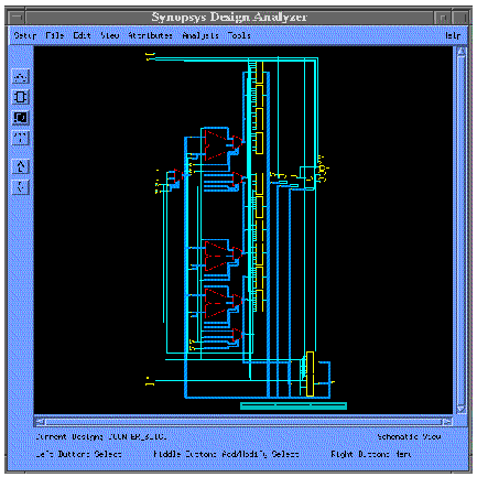
Analyze the design and then Elaborate it. You will get a design as shown in figure 28.
4.3.2.1- Test Bench for 3 digit Counter:
For the simulation of 3 digit Counter, a test bench has been generated by connecting CLOCK and COUNTER_3DIGIT together (figure 29), as given below. Save it in file BENCH_COUNTER_3DIGIT.vhd.
Fig 28: 3 digit Counter
Fig 29: Test bench of 3 digit BCD Counter
library IEEE;
use IEEE.STD_LOGIC_1164.all;
entity BENCH_COUNTER_3DIGIT is
generic (
HALF_PERIOD : time := 5 ns);
end BENCH_COUNTER_3DIGIT;
architecture STRUCTURE of BENCH_COUNTER_3DIGIT is
-- Component declarations
component CLOCK
generic (
HALF_PERIOD : time := 5 ns);
port (
CP : out STD_LOGIC);
end component;
component COUNTER_3DIGIT
port (
CP, RESET : in STD_LOGIC;
COUNT : buffer STD_LOGIC_VECTOR(11 downto 0));
end component;
-- Configuration specifications
for CLK1 : CLOCK use entity WORK.CLOCK(BEHAVIOR);
for CUNTR3 : COUNTER_3DIGIT use entity
WORK.COUNTER_3DIGIT(ALGORITHM);
-- Signal declarations
signal CP, RESET : STD_LOGIC;
signal COUNT : STD_LOGIC_VECTOR(11 downto 0);
signal STOP : BOOLEAN;
begin
-- Component Instantiations using positional association
CLK1 : CLOCK generic map(HALF_PERIOD)
port map(CP);
CUNTR3 : COUNTER_3DIGIT port map(CP, RESET, COUNT);
RESETTING : process
begin
wait on CP;
RESET <= '0';
for I in 1 to 2 loop
for I in 1 to 2 loop
wait for HALF_PERIOD;
end loop;
RESET <= not RESET;
end loop;
-- To stop the process
wait until STOP'event;
end process;
end STRUCTURE;
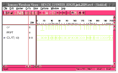
Analyze the bench and then simulate it. In the Command line of Synopsys VHDL Debugger (Vhdldbx) window, type:
# trace CP RESET COUNT
# run 200
You will get simulation result as shown in figure 30.
Fig 30: Simulation results of test bench of 3 digit Counter
4.4- MULTIPLIER
In this part, first a Dataflow model of an unsigned 4x4 bit Multiplier is given. Then an unsigned 8x8 bit Multiplier is designed using Algorithmic modeling style. In the end, a signed 8x8 bit Multiplier is designed.
4.4.1- Unsigned 4x4 Bit Multiplier:
A Dataflow description of an unsigned 4x4 bit Multiplier, using conditional concurrent signal assignment statements, is given below. Save it in file UNSIGNED_MULT4x4.vhd.
library IEEE;
use IEEE.STD_LOGIC_1164.all;
use IEEE.STD_LOGIC_UNSIGNED.all;
entity UNSIGNED_MULTIPLIER4x4 is
port (
IN1, IN2 : in STD_LOGIC_VECTOR(3 downto 0);
PRODUCT : out STD_LOGIC_VECTOR(7 downto 0));
end UNSIGNED_MULTIPLIER4x4;
architecture DATA_FLOW of UNSIGNED_MULTIPLIER4x4 is
signal PP0, PP1, PP2, PP3 : STD_LOGIC_VECTOR(7 downto 0);
-- These will hold shifted partial products
constant ZERO : STD_LOGIC_VECTOR := "00000000";
begin
PP0 <= ("0000" & IN1) when IN2(0) = '1' else
ZERO;
PP1 <= ("000" & IN1 & '0') when IN2(1) = '1' else
ZERO;
PP2 <= ("00" & IN1 & "00") when IN2(2) = '1' else
ZERO;
PP3 <= ('0' & IN1 & "000") when IN2(3) = '1' else
ZERO;
PRODUCT <= (PP3 + PP2) + (PP1 + PP0);
end DATA_FLOW ;
Analyze the code and then simulate it. After elaboration, you will get a design as shown in figure 31.
Fig 31: Unsigned 4x4 bit Multiplier
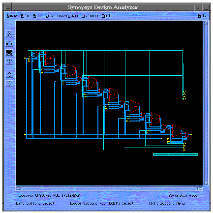
4.4.2- Unsigned 8x8 Bit Multiplier:
An Algorithmic description of an unsigned 8x8 bit Multiplier is given below. Save it in file UNSIGNED_MULT8x8.vhd.
library IEEE;
use IEEE.STD_LOGIC_1164.all;
use IEEE.STD_LOGIC_UNSIGNED.all;
entity UNSIGNED_MULTIPLIER8x8 is
port (
IN1, IN2 : in STD_LOGIC_VECTOR(7 downto 0);
PRODUCT : out STD_LOGIC_VECTOR(15 downto 0));
end UNSIGNED_MULTIPLIER8x8;
architecture ALGORITHM of UNSIGNED_MULTIPLIER8x8 is
begin
MULT_PROCESS : process(IN1, IN2)
variable SUM : STD_LOGIC_VECTOR(15 downto 0);
begin
SUM := "0000000000000000";
SHIFT_ADD_LOOP : for I in 7 downto 0 loop
if IN2(I) = '1' then
SUM := SUM + ("00000000" & IN1);
-- Computation of partial products
end if;
if I /= 0 then
SUM := SUM(14 downto 0) & '0';
-- Left shifting of sum
end if;
end loop SHIFT_ADD_LOOP;
PRODUCT <= SUM;
end process MULT_PROCESS;
end ALGORITHM;
Analyze the code and then simulate it. After elaboration, you will get a design as shown in figure 32.
4.4.3- Signed 8x8 Bit Multiplier:
An Algorithmic description of a signed 8x8 bit Multiplier is given below. Save it in file SIGNED_MULT8x8.vhd.
package PACK is
-- Type declarations
subtype INPUT_TYPE is INTEGER range -128 to 127;
Fig 32: Unsigned 8x8 bit Multiplier
subtype OUTPUT_TYPE is INTEGER range -32768 to 32767;
end PACK;
library IEEE;
use IEEE.STD_LOGIC_1164.all;
use WORK.PACK.all;
entity MULTIPLIER8x8 is
port (
CP, RESET : in STD_LOGIC;
IN1, IN2 : in INPUT_TYPE;
PRODUCT : out OUTPUT_TYPE);
end MULTIPLIER8x8;
architecture ALGORITHM of MULTIPLIER8x8 is
begin
process
variable I1, I2 : INPUT_TYPE;
variable PROD : OUTPUT_TYPE;
begin
RESET_LOOP : loop
I1 := 0;
I2 := 0;
PRODUCT <= 0;
I1 := IN1;
I2 := IN2;
wait until ( CP = '1' and CP'event);
if RESET = '1' then
exit RESET_LOOP;
end if;
MAIN_LOOP : loop
PROD := I1 * I2;
PRODUCT <= PROD;
wait until ( CP = '1' and CP'event);
if RESET = '1' then
exit RESET_LOOP;
end if;
end loop MAIN_LOOP;
end loop RESET_LOOP;
end process;
end ALGORITHM;
Two subtypes INPUT_TYPE and OUTPUT_TYPE of predefined type INTEGER are declared in package PACK, which is declared and used in the above file.
Analyze the code and then elaborate it, you will get a design as shown in figure 33.
4.4.3.1- Test Vector for Signed 8x8 Multiplier:
For the simulation of Signed 8x8 bit Multiplier, a test vector is given below save it in file
TEST_MULTIPLIER.
Fig 33: Signed 8x8 bit Multiplier
trace CP RESET IN1 IN2 PRODUCT
assign '0' /MULTIPLIER8x8/CP
assign '0' /MULTIPLIER8x8/RESET
assign 10 /MULTIPLIER8x8/IN1
assign (-10) /MULTIPLIER8x8/IN2
run 10
assign '1' /MULTIPLIER8x8/CP
run 10
assign '0' /MULTIPLIER8x8/CP
assign '1' /MULTIPLIER8x8/RESET
run 10
assign '1' /MULTIPLIER8x8/CP
assign 2 /MULTIPLIER8x8/IN1
assign 3 /MULTIPLIER8x8/IN2
run 10
assign '0' /MULTIPLIER8x8/CP
assign '0' /MULTIPLIER8x8/RESET
run 10
assign '1' /MULTIPLIER8x8/CP
run 10
assign '0' /MULTIPLIER8x8/CP
assign '1' /MULTIPLIER8x8/RESET
run 10
assign '1' /MULTIPLIER8x8/CP
assign (-128) /MULTIPLIER8x8/IN1
assign (-128) /MULTIPLIER8x8/IN2
run 10
assign '0' /MULTIPLIER8x8/CP
assign '0' /MULTIPLIER8x8/RESET
run 10
assign '1' /MULTIPLIER8x8/CP
run 10
assign '0' /MULTIPLIER8x8/CP
assign '1' /MULTIPLIER8x8/RESET
run 10
assign '1' /MULTIPLIER8x8/CP
assign 127 /MULTIPLIER8x8/IN1
assign 127 /MULTIPLIER8x8/IN2
run 10
assign '0' /MULTIPLIER8x8/CP
assign '0' /MULTIPLIER8x8/RESET
run 10
assign '1' /MULTIPLIER8x8/CP
run 10
assign '0' /MULTIPLIER8x8/CP
assign '1' /MULTIPLIER8x8/RESET
run 10
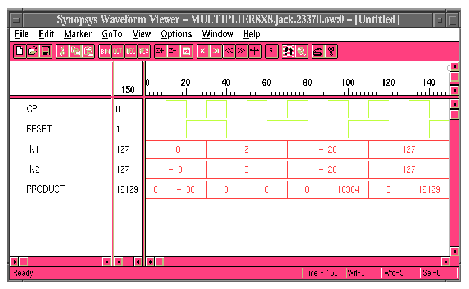
Now simulate the Signed 8x8 Multiplier. Command line of Synopsys VHDL Debugger (Vhdldbx) window, type:
You will get a simulation results as shown in figure 34.
